Jumper settings, Chapter 3, Motherboard information – Lanner MR-730 User Manual
Page 14
11
Motherboard Information
Chapter 3
Network Application Platforms
Jumper Settings
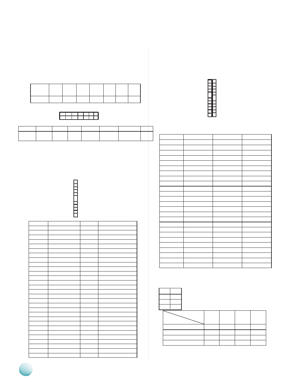
JTAG(JTAG1): The Jtag is a debug port provided
as a means for testing the main board and looking for
possibility of field faults. It can also be used for flash
writing.
Mini-PCI Connector (MPCIE1): The 58-pin Mini-
PCIe slot enables a Mini-PCIe expansion module to be
connected to the board. For example, a WiMAX/WiFi
module.
CompactFlash Connector (CF1): It is for connecting a
Compact Flash card to be served as your system’s storage.
The connector is a CF Type II slot which could fit both CF
Type I or CF Type II cards.
CPU Clock Speed Adjustment Dip Switch (SW1)
1
2
.
.
.
.
.
58
26
.
.
.
.
.
50
1
.
.
.
.
.
25
PIN NO.
1
3
5
7
9
11
13
Function
EJTG_
TRST#
TDI
TDO
JTG_TMS JTG_TCK EJTAG_RST
NC
Function
GND
GND
GND
GND
GND
NC
3.3V
PIN NO.
2
4
6
8
10
12
14
1 3 5 7 9 1 1 1 3
2 4 6 8 1 0 1 2 1 4
PIN NO.
FUNCTION
PIN NO.
FUNCTION
1
2
3.3V
3
4
GND
5
6
1.5V
7
8
9
GND
10
11
CLK_PCIE_N
12
13
CLK_PCIE_P
14
15
GND
16
17
18
GND
19
20
21
GND
22
23
PCIE_RX_N
24
25
PCIE_RX_P
26
GND
27
GND
28
1.5V
29
GND
30
31
PCIE_TX_N
32
33
PCIE_TX_P
34
GND
35
GND
36
USB-
37
38
USB+
39
40
GND
41
42
43
44
45
46
47
48
1.5V
49
50
GND
51
52
3.3V
53
GND
54
GND
55
GND
56
GND
57
GND
58
GND
Pin No.
Function
Pin No.
Function
1
GND
26
NA
2
DATA3
27
DATA10
3
DATA4
28
DATA12
4
DATA5
29
DATA13
5
DATA6
30
DATA14
6
DATA7
31
DATA15
7
CE1#
32
CE2#
8
A10
33
VS1#
9
OE#
34
IOR#
10
A9
35
IOW#
11
A8
36
WE#
12
A7
37
READY#
13
CFVCC3
38
CFVCC3
14
A6
39
CSEL
15
A5
40
VS2#
16
A4
41
RESET
17
A3
42
WAIT#
18
A2
43
INPACK#
19
A1
44
REG#
20
A0
45
DASP#
21
DATA0
46
DIAG#
22
DATA1
47
DATA8
23
DATA2
48
DATA9
24
WP
49
DATA10
25
NA
50
GND
1
2
3
4
ON
Function
Dip Switch Selector
750
MHz
700
MHz
600
MHz
500
MHz
1
ON
ON
ON
ON
2
ON
ON
ON
OFF
3
ON
ON
OFF
ON
4
ON
OFF
OFF
OFF
OFF