Jumper settings, Chapter 3, Motherboard information – Lanner MR-301 User Manual
Page 12
9
Motherboard Information
Chapter 3
Network Application Platforms
Jumper Settings
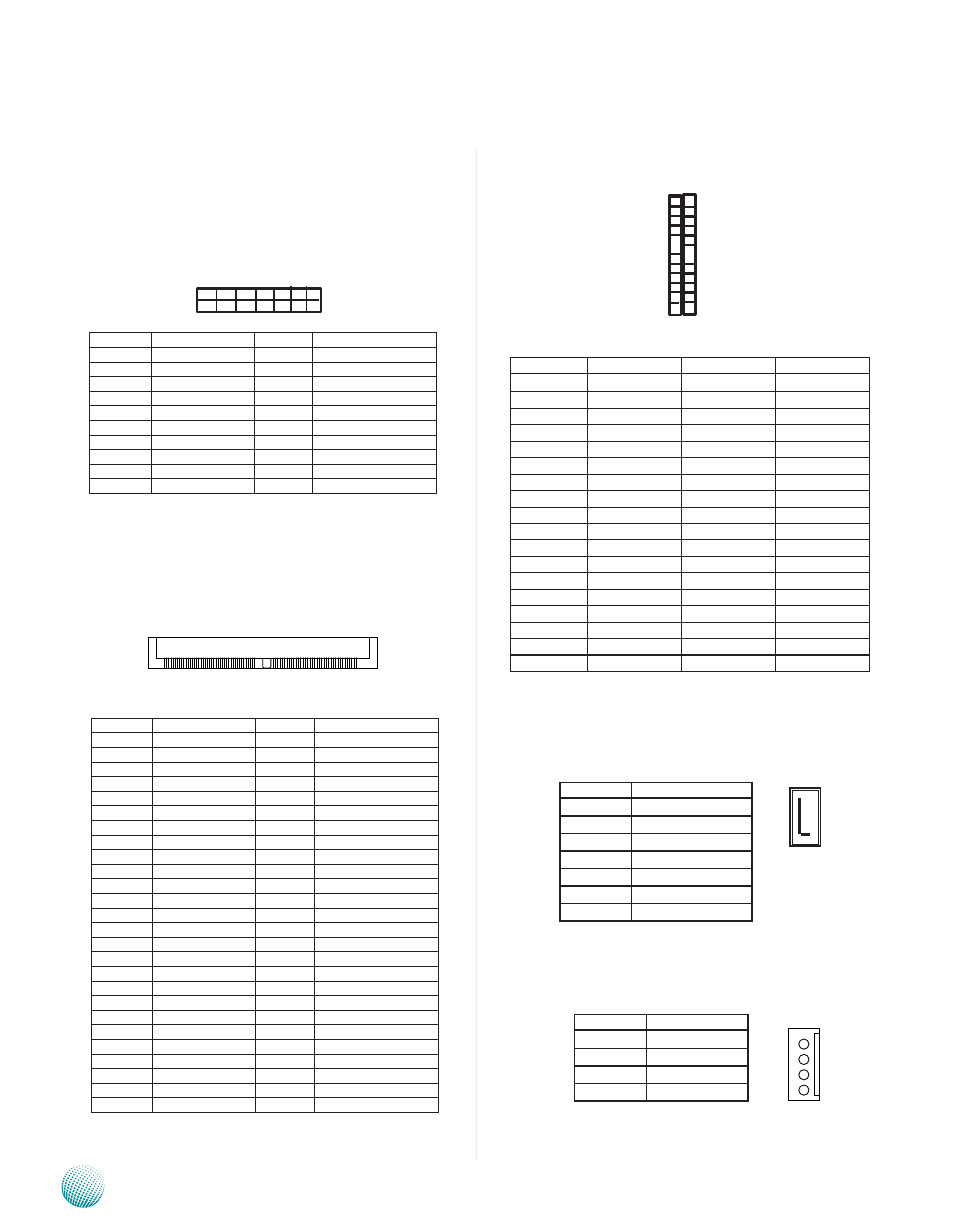
88F6281 JTAG Connector (J9): The Jtag is a debug
port provided as a means for testing the main board and
looking for possibility of field faults. It can also be used for
flash writing.
Mini-PCIe Connector (MPCIE2): The 52-pin Mini-
PCIe slot enables a Mini-PCIe expansion module to be
connected to the board. For example, a WiMAX/WiFi
module.
PCI-E X 1 Golden Finger Connector (PCIE2)
SATA Driver Connector (J12): It is for connecting
a 2.5’’ SATA harddisk to be served as your system’s
storage. The system can support up to1 disk of 2.5” in
maximum.
Serial-ATA Power Connector (CON1, CON2): It is
used for connectig the SATA power cord.
26
.
.
.
.
.
50
1
.
.
.
.
.
25
PIN NO.
FUNCTION
PIN NO.
FUNCTION
1
WAKE1-
2
V_3.3
3
NC
4
GND
5
NC
6
V_1.5
7
CLKREQ-
8
NC
9
GND
10
NC
11
Clk_MiniPex_n
12
NC
13
Clk_MiniPex_p
14
NC
15
GND
16
NC
17
NC
18
GND
19
NC
20
NC
21
GND
22
Rst#_Sys
23
MiniP_R_n
24
V_3.3
25
MiniP_R_p
26
GND
27
GND
28
V_1.5
29
GND
30
MPE_SMCLK
31
MiniP_T_n
32
MPE_SMDTA
33
MiniP_T_p
34
GND
35
GND
36
NC
37
NC
38
NC
39
NC
40
GND
41
NC
42
NC
43
NC
44
NC
45
NC
46
NC
47
NC
48
V_1.5
49
NC
50
GND
51
NC
52
V_3.3
Pin No.
Function
Pin No.
Function
A1
NC
B1
V_12
A2
V_12
B2
V_12
A3
V_12
B3
V_12
A4
GND
B4
GND
A5
NC
B5
NC
A6
NC
B6
NC
A7
GND
B7
GND
A8
GND
B8
V_3.3
A9
V_3.3
B9
NC
A10
V_3.3
B10
V_3.3
A11
Rst#_Sys
B11
NC
A12
GND
B12
NC
A13
Clk_Pex_p
B13
GND
A14
Clk_Pex_n
B14
PciE_T_p
A15
GND
B15
PciE_T_n
A16
PciE_R_p
B16
GND
A17
PciE_R_n
B17
NC
A18
GND
B18
GND
20 18 16 14 12 10 8 6 4 2
19 17 15 13 11 9 7 5 3 1
PIN NO.
FUNCTION
PIN NO.
FUNCTION
1
V_3.3
2
V_3.3
3
Jt_Reset#
4
GND
5
Jt_Tdi
6
GND
7
Jt_Tms_CPU
8
GND
9
Jt_Clk
10
GND
11
Jt_Clk
12
GND
13
Jt_Tdo
14
GND
15
Jt_Srst#
16
GND
17
NC
18
GND
19
NC
20
GND
MPCIE2
Pin No.
Description
1
GND
2
Sata0_Tx_p
3
Sata0_Tx_n
4
GND
5
Sata0_Rx_n
6
Sata0_Rx_p
7
GND
1
2
3
4
5
6
7
1
2
3
4
Pin No.
Description
1
V_12
2
GND
3
GND
4
V_5