Chapter 3, Motherboard information – Lanner FW-7581 User Manual
Page 13
10
Motherboard Information
Chapter 3
Network Application Platforms
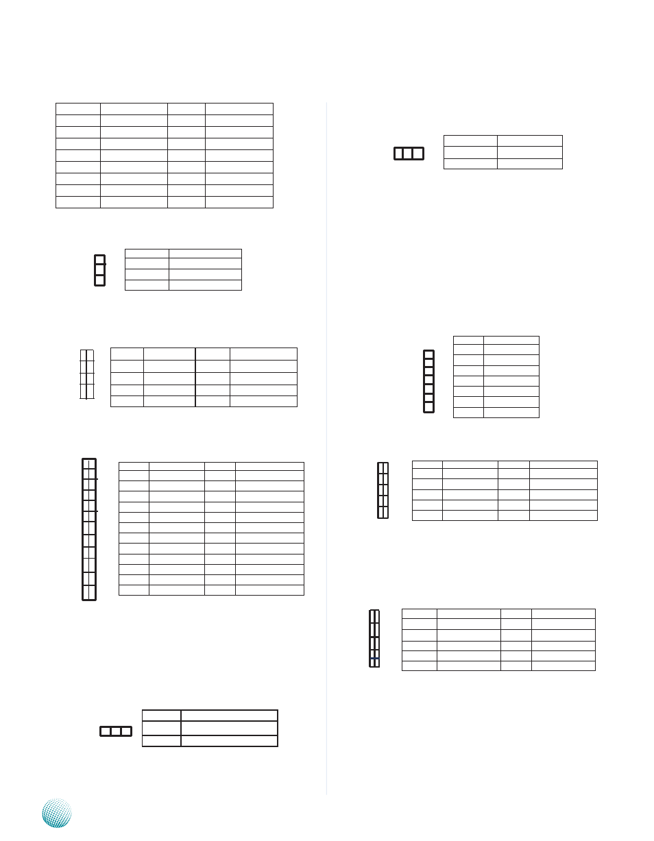
PIN
DESCRIPTION PIN
DESCRIPTION
18
A2
43
INPACK#
19
A1
44
REG#
20
A0
45
DASP#
21
DATA0
46
DIAG#
22
DATA1
47
DATA8
23
DATA2
48
DATA9
24
WP
49
DATA10
25
CD2-
50
GND
CF Master/Slave Selection Jumper(J2): It is for selecting
the CF card as a master or slave drive.
Keyboard and mouse interface Connectors(J16): A 2x4
(2.54mm) pin header for connecting the PS/2 keyboard
and mouse interface cable.
Front LCD Module Connector(J15): A 2x5 pin header for
connecting the front system LCD display.
Hardware or Software Reset Jumper(J14): The jumper
can be adjusted to be in either hardware or software reset
mode when the reset switch is pressed. The hardware
reset will reboot the system without turning off the power.
The software reset can be programmed to reset a software
to its default settings.
Clear CMOS jumper (J5): It is for clearing the CMOS
memory and system setup parameters by erasing the data
stored in the CMOS RAM such as the system passwords.
DIMM Socket (DIMM1, DIMM2): The 240-pin DDR3 SO-
DIMM is for connecting the DDR3 1066/1333 memory.
The system can support up to 4 GB in maximum and
Dual-channel architecture. Dual channel doubles data
throughput from the memory to the memory controller
by maximize memory throughput from 64-bit buses to
128-bit bus.
SATA 1 and 2 Connectors (J3, J4): It is for connecting a
2.5’’ SATA hard disk to be served as your system’s storage.
The system can support a maximum of 2 disks. It conforms
with SATA II (3.0 Gbs).
Serial Interface Connectors(J13, COM2): A 10-pin header
for connecting the RS-232 serial port module cable.
SPI-ROM Update Connector (SPI-ROM1): Using the
appropriate cable to connect this 10-pin ISP in header
connector, the SPI Flash soldered on board can be
updated.
LPC I/O bus (Port 80) (LPC1): It is a proprietary connector
for connecting a checkpoint device to output checkpoints
throughout bootblock and Power-On Self Test (POST) to
indicate the task the system is currently executing.
2
4
6
8
10
1
3
5
7
9
3 2 1
Pin No.
Function
PIN NO.
DESCRIPTION
1
DCD#
2
DSR
3
SIN
4
RTS#
5
SOUT
6
CTS#
7
DTR#
8
RI#
9
GND
10
KEY
Pin No.
Function
Pin No.
Function
1
NC
2
NC
3
ICH_SPI_CS0#
4
V_3P3_SPI_R
5
SB_SPI_MISO
6
SPI_HD_N
7
KEY
8
ICH_SPI_CLK
9
GND
10
ICH_SPI_MOSI
1
3
5
7
9
2
4
6
8
10
Pin No.
Function
PIN NO.
DESCRIPTION
1
P5V
2
GND
3
LPT17
4
VEE
5
LPT14
6
LPT16
7
LPT3
8
LPT2
9
LPT5
10
LPT4
11
LPT7
12
LPT6
13
LPT9
14
LPT8
15
LCD-
16
P5V
17
KPA1
18
KPA2
19
KPA3
20
KPA4
21
LCM_RST
22
CTR_GRN
23
CTR_RED
24
HDD_LED¬
24
22
20
18
16
14
12
10
8
6
4
2
23
21
19
17
15
13
11
9
7
5
3
1
Pin No.
Function
PIN NO. DESCRIPTION
1
P5V_KM
2
MSCLK
3
MSDATA
4
KEY
5
KBDATA
6
KEY
7
KGND
8
KBCLK
7
5
3
1
8
6
4
2
3 2 1
Pin No.
Function
1
GND
2
TX_P
3
TX_N
4
GND
5
RX_N
6
RX_P
7
GND
7
6
5
4
3
2
1
3
2
1
Pin No.
Function
1
NC
2
MST_SLV
3
GND
Pin No.
Function
1-2
Hardware reset
2-3
Software reset
Pin No.
Function
1-2
Normal (Default)
2-3
Clear CMOS