Chapter 3, Board layout – Lanner LVC-5770 User Manual
Page 25
25
Board Layout
Chapter 3
Embedded and Industrial Computing
MPCIE1: Mini-PCIe Connector with one SIM Card
Reader(SIM1). It supports both Wi-Fi and 3G module.
Both USB and PCIe signal card type can be used on the
connector.
Pin
Signal
Pin
Signal
1
WAKE#
2
VCC3.3
3
N/A
4
GND
5
N/A
6
VCC1.5
7
CLKREQ#
8
USIM_PWR
9
GND
10
UIM_DATA
11
PCIE_CLK_N3
12
UIM_CLK
13
PCIE_CLK _P3
14
UIM_RESET
15
GND
16
UIM_VPP
17
RSV
18
GND
19
RSV
20
N/A
21
GND
22
PLTRST
23
PCIE_RX_N3
24
VCC3.3
25
PCIE_RX_P3
26
GND
27
GND
28
VCC1.5
29
GND
30
SMBCLK
31
PCIE_TX_N3
32
SMBDATA
33
PCIE_TX_P3
34
GND
35
GND
36
USB_N8
37
GND
38
USB_P8
39
VCC3.3
40
GND
41
VCC3.3
42
N/A
43
GND
44
N/A
45
RSV
46
N/A
47
RSV
48
VCC1.5
49
RSV
50
GND
51
RSV
52
VCC3.3
MPCIE2: Mini-PCIe Connector. It does not come with a
SIM card reader so only Wi-Fi modules are supported.
Both USB and PCIe signal card type can be used on the
connector.
Pin
Signal
Pin
Signal
1
WAKE#
2
VCC3.3
3
N/A
4
GND
5
N/A
6
VCC1.5
7
CLKREQ#
8
N/A
9
GND
10
N/A
11
PCIE_CLK _N4
12
N/A
13
PCIE_CLK _P4
14
N/A
15
GND
16
N/A
17
RSV
18
GND
19
RSV
20
N/A
21
GND
22
PLTRST
23
PCIE_RX_N4
24
VCC3.3
25
PCIE_RX_P4
26
GND
27
GND
28
VCC1.5
29
GND
30
SMBCLK
31
PCIE_TX_N4
32
SMBDATA
33
PCIE_TX_P4
34
GND
35
GND
36
USB_N9
37
GND
38
USB_P9
39
VCC3.3
40
GND
41
VCC3.3
42
N/A
43
GND
44
N/A
45
RSV
46
N/A
47
RSV
48
VCC1.5
49
RSV
50
GND
51
RSV
52
VCC3.3
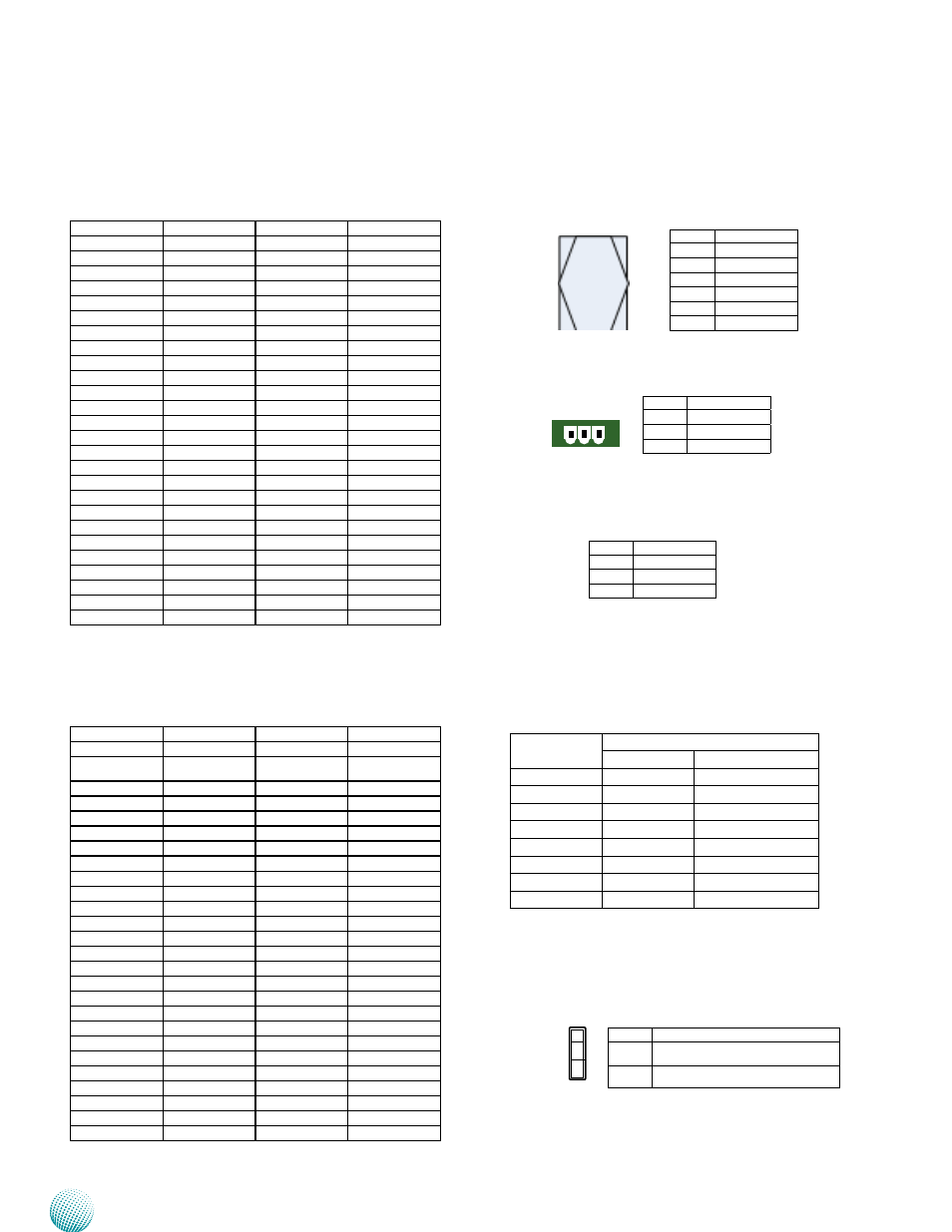
SIM Card Socket (SIM1):
CN3: A power connector with power -ignition Control
DCJK1 (Optional): An optional DC Jack type of Power
Connector
LAN1/LAN2 Ports (LAN1/LAN2): The LAN ports are
provided by Intel 82574L Ethernet controller whose
interface complies with PCI-e 1.1 (2.5 Ghz). It has advanced
management features including IPMI pass-through via
SMBus or NC-SI, WOL, PXE remote boot, ISCSI boot and
VLAN filtering.
Pin No.
Description
Fast Ethernet Gigabit Ethernet
1
TX+
BI_DA+
2
TX-
BI_DA-
3
RX+
BI_DB+
4
--
BI_DC+
5
--
BI_DC-
6
RX-
BI_DB-
7
--
BI_DD+
8
--
BI_DD-
Enable or Disable Daughter Board LEK-IOA7 (COMSLT1):
This jumper is for enabling or disabling COM3/COM4
daughter board LEK-IOA7.
Pin No.
Pin Name
1
Ignition
2
GND
3
DC_VIN
Pin No.
Pin Name
1
DC_VIN
2
GND
3
GND
1 2 3
Pin No.
Pin Name
1-2
Disable
2-3
Enable
1
2
3
Pin No.
Description
C1
UIM_PWR
C2
UIM_RST
C3
UIM_CLK
C5
GND
C6
UIM_VPP
C7
UIM_DAT
C5 C7
C1 C3