Chapter 3, Board layout – Lanner LVC-5770 User Manual
Page 21
21
Board Layout
Chapter 3
Embedded and Industrial Computing
Switch
Protocol
SCT1
SCT3
RS-232 (default)
1-2
1-5, 2-6, 3-7, 4-8
(default)
RS-422
3-4
5-9, 6-10, 7-11, 8-12
RS-485
5-6
5-9, 6-10, 7-11, 8-12
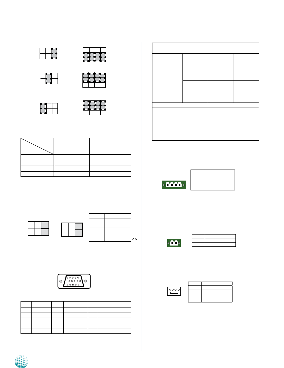
J13, J14: Select COM1 and COM2 Pin9 Function (in
RS-232) respectively. The Ring indicator pinout of the RS-
232 COM port can be altered according to the following
jumper settings.
Digital Input and Output (MIO, J15): A DE-15 Male
Connector for 4 DI & 3 DO, 12V
Pin
Signal
Pin
Signal
Pin
Signal
1
RIO_IN0
6
RIO_OUT0 11 EXT_POWER_ON
2
RIO_IN1
7
RIO_OUT1 12
IGN_IN0
3
RIO_IN2
8
RIO_OUT2 13
IGN_IN1
4
RIO_IN3
9
RIO_OUT3 14
GND
5
GND
10
GND
15
12V_OUT (1A)
Maximum input/output current for each port is
100mA
For all Input/
output pins:
Voltage
Logic
Register
Di: <0.8V
Do: <0.4V
Low
0
DI: 0.9 ~ 5V
Do:5V
High
1
The default BIOS value is 1 for DI and 1 for DO
Pin 11 is used for remote power switch.
1.
Pin 6 is used for relay power switch.
2.
Pin12 and pin13 can be used for DI wake-up
3.
function (Refer to the flow chart in Chapter 4 and
the ISM in Appendix A).
DC_in and out (CN4) : 9~36V DC power input and output
Integrated in a 4-pin terminal.
48V DC_IN for PoE Power Supply (CN3):
Optional Connector (CN1):
9
5
1
12
8
4
9
5
1
12
8
4
9
5
1
12
8
4
1
2
5
6
5
6
1
2
5
6
1
2
Pin No.
Function
1-2
Supply +5V to
the Device
3-4
Supply +12V to
the Device
5-6
Ring-in (default)
2
1
J13
J14
6
5
2
1
6
5
15 11
5 1
Pin No.
Function
1
P930V_IN
2
P930V_GND
3
GND_930V
4
P930V_OUT
Pin No.
Function
1
GND
2
48V_IN
4 3 2 1
2 1
4 3 2 1
CN1
Pin No.
Function
1
VCC12
2
GND
3
GND
4
VCC5