Sundance FC201 User Manual
Page 3

Page 3 of 3
Revision 0.4
Sundance Digital Signal Processing Inc.
4790 Caughlin Parkway 233, Reno, NV 89519-0907, U.S.A.
Tel: +1 (775) 827-3103, Fax: +1 (775) 827-3664, email:
www.sundancedsp.com
1.
GENERAL DESCRIPTION
This document describes the specifications of a 3L Diamond/FPGA firmware module.
The FC201 is an efficient implementation of a general offset/gain/delay correction. In order for
it to be used within a Diamond/FPGA system, the I/O interfaces are ‘standardized’ to the model
described by Diamond
1
.
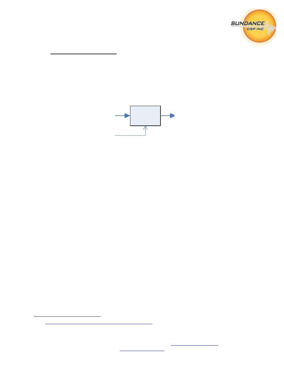
FC201
ADC_OUT
ADC_IN
COEFF_IN
Figure 1 - Component Diagram
The firmware module operates in a flow-through mode; for every ADC_IN sample written, one
ADC_OUT sample will be clocked out.
The FC201 firmware module is designed to correct a single digital data channel. Typically, each
channel requires its own correction coefficients. Coefficients are loaded asynchronously and are
applied prior to the next input cycle. Loading coefficients affects a reset of the module. The
module will not accept ADC_IN samples until the first set of coefficients are loaded.
The module is useful for correcting ADC input as well as DAC output data streams.
1
See:
http://www.3l.com/Diamond/Documentation/Diamond.pdf
(Chapter 28, “FPGA Tasks”)
