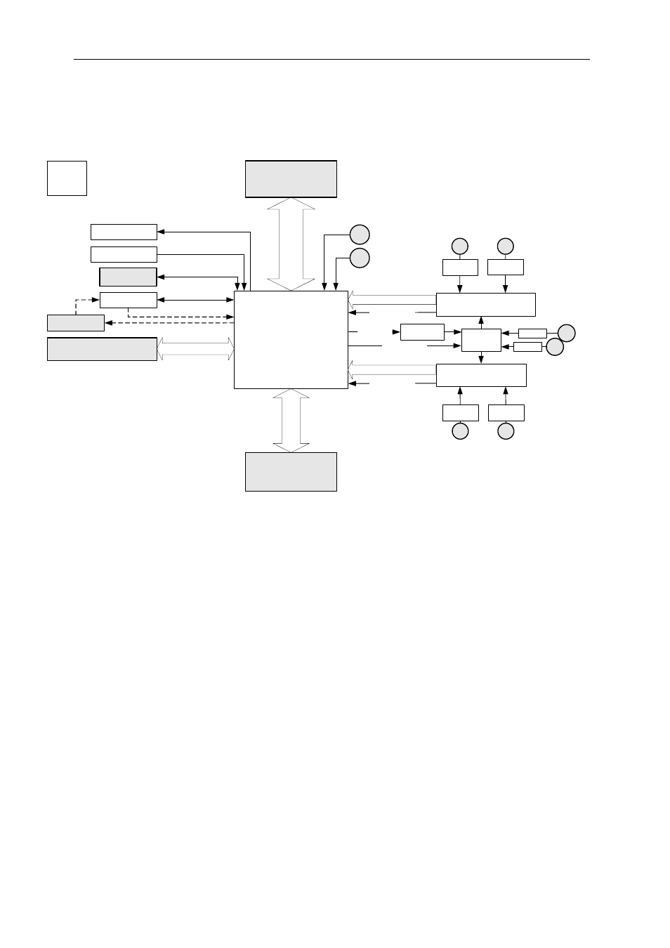
Block diagram - architecture, Figure 1 - block diagram – Sundance SMT364 User Manual
Page 7
Version 1.0
Page 7 of 37
SMT364 User Manual
Block Diagram - Architecture.
The following diagram shows the architecture of the SMT364.
Bo
ard R
e
s
e
t
2x
C
o
mm-
Po
rt
/S
DL
24 I/O pins
Xilinx FPGA
Virtex-II, FG456
XC2V1000-4
324 I/O Pins
1.5V Core
3.3V I/O
J2 Bottom Primary TIM
Connector
2x CommPorts/SDLs 1 & 4
J1 Top Primary TIM
Connector
2x CommPorts/SDLs 0 & 3
#1
120 I/O pins
AC or DC
coupling*
2xAD6645 ADCs (A and B)
14-bit @ 105MSPS
52-pin LQFP
30 I/O pins; 28-bit data; ctl
2xAD6645 ADCs (C and D)
14-bit @ 105MSPS
52-pin LQFP
#2
Clock feedback
Trig
1
Trig
2
6-pin JTAG
header
On-board Oscillator
50 MHz
4 LEDs or
4 LVTTL I/O pins
FPGA PROM
XC18V04
Clock
Multiplexer
Clock
parameters
3 Power
supply
LEDs
‘FPGA configured’
LED
Clock feedback
Clk
1
Filter
Filter
2xClock
synthesizers
Clk
2
Clock selection
2 Sundance High-speed
Bus connector: 2 x 60 bits
AC or DC
coupling*
JTAG chain
* Option to the board
#3
AC or DC
coupling*
#4
AC or DC
coupling*
30 I/O pins; 28-bit data; ctl
Figure 1 - Block Diagram.
Connections to the outside world are greyed out.
Main parts of the board are described in the next part of this document.