Crosstalk, Crosstalk -6 – Measurement Computing PCI-DAS64/M2/16 User Manual
Page 27
PCI-DAS64/M2/16 User's Guide
Specifications
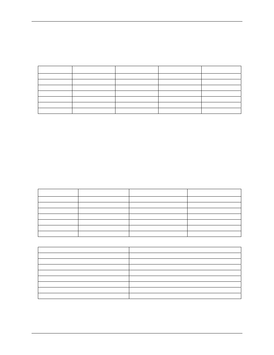
Typical accuracy is derived directly from the various component typical errors. The information in
assumes that each of the errors contributes in the same direction.
Table 5. Analog input — accuracy components specifications
Range
Gain error
Offset error
DLE
ILE
±5.000 V
±3.0 max, ±2.0 typ
±3.0 max, ±2.0 typ
±1.0 max, ±0.5 typ
±2 max, ±1.0 typ
±2.500 V
±3.0 max, ±2.0 typ
±5.0 max, ±4.0 typ
±1.0 max, ±0.5 typ
±2 max, ±1.0 typ
±1.250 V
±3.0 max, ±2.0 typ
±5.0 max, ±4.0 typ
±1.0 max, ±0.5 typ
±2 max, ±1.0 typ
±0.625 V
±5.0 max, ±4.0 typ
±5.0 max, ±4.0 typ
±1.0 max, ±0.5 typ
±2 max, ±1.0 typ
0 to + 5.000 V
±4.0 max, ±3.0 typ
±4.0 max, ±3.0 typ
±1.0 max, ±0.5 typ
±2 max, ±1.0 typ
0 to + 2.500 V
±6.0 max, ±5.0 typ
±5.0 max, ±4.0 typ
±1.0 max, ±0.5 typ
±2 max, ±1.0 typ
0 to + 1.250 V
±6.0 max, ±5.0 typ
±5.0 max, ±4.0 typ
±1.0 max, ±0.5 typ
±2 max, ±1.0 typ
As shown in Tab
, total board error is a combination of gain, offset, differential linearity error (DLE), and
integral linearity error (ILE). The theoretical worst-case error of the board can be calculated by summing these
component errors. Worst-case errors are realized only in the unlikely event that each of the component errors
are at their maximum level, and causing error in the same direction.
Crosstalk
Crosstalk is defined here as the influence of one channel upon another when scanning two channels at the
maximum rate. A full-scale 100 Hz triangle wave is input on channel 1, and channel 0 is tied to analog ground
at the 100-pin user connector. Tabl
summarizes the influence of channel 1 on channel 0 with the effects of
noise removed. The residue on channel 0 is described in LSBs.
Table 6. Crosstalk specifications
Range Crosstalk
(LSB
pk-pk
)
Per channel rate (kS/s)
ADC rate (kS/s)
±5.000 V
15
750
1500
±2.500 V
15
750
1500
±1.250 V
20 750
1500
±0.625 V
8 375 750
0 V to + 5.000 V
15 750
1500
0 V to + 2.500 V
20 750
1500
0 V to + 1.250 V
8 375 750
Table 7. Analog input drift specifications
Analog input full-scale gain drift
+0.3 LSB/°C typical
Analog input zero drift
+2.1 LSB/°C typical
Overall analog input drift
±2.4 LSB/°C typical
Common mode range
±5 V
CMRR @ 60Hz
-90 dB
Input leakage current
2.3 nA
Input impedance
10 x 10
11
Ω
Absolute maximum input voltage
±15 V
Warm-up time
60 minutes
6-6