Noise performance, Analog input calibration, Analog output – Measurement Computing USB-202 User Manual
Page 15
USB-202 User's Guide
Specifications
15
Noise performance
For the peak to peak noise distribution test, the input channel is connected to AGND at the input terminal block,
and 12,000 samples are acquired at the maximum throughput.
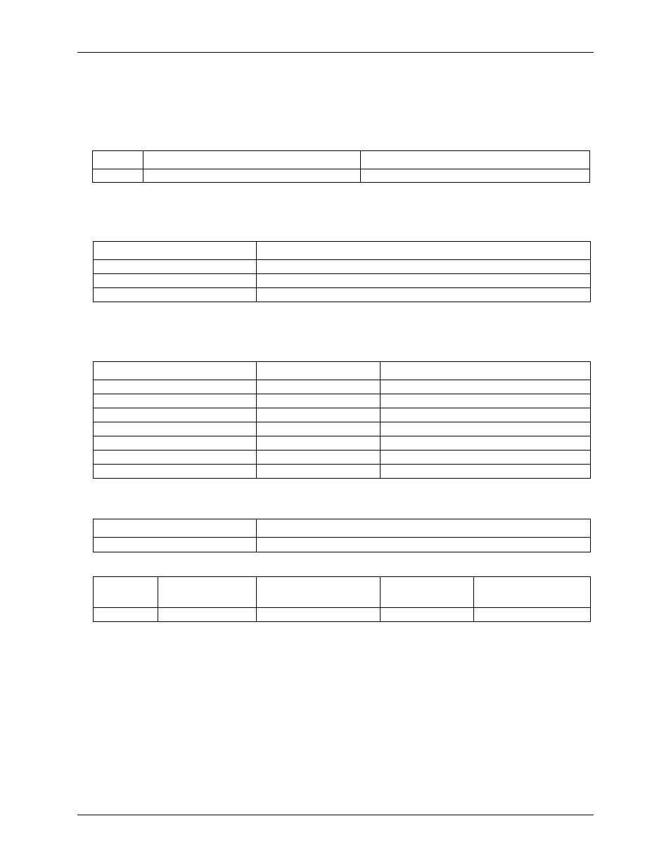
Table 3. Noise performance specifications
Range
Counts
LSBrms
±10 V
5
0.76
Analog input calibration
Table 4. Analog input calibration specifications
Parameter
Specification
Recommended warm-up time
15 minutes min
Calibration method
Factory
Calibration interval
1 year
Analog output
Table 5. Analog output specifications
Parameter
Condition
Specification
Resolution
12 bits, 1 in 4,096
Output range
0 V to 5.0 V
Number of channels
2
Throughput (Note 1)
Software paced
250 S/s single channel typ, PC dependent
Power on and reset voltage
Initializes to 000h code
0 V, ±10 mV
Output drive
Each D/A OUT
5 mA, sourcing
Slew rate
0.8 V/ µs typ
Note 1:
Maximum throughput when scanning is machine dependent.
Table 6. Analog output accuracy, all values are (±); accuracy tested at no load
Range
Accuracy (LSB)
0 V to 5.0 V
5.0 typ, 45.0 max
Table 7. Analog output accuracy components, all values are (±)
Range
% of FSR
Gain Error at FS (mV)
Offset (mV)
(Note 2)
Accuracy at FS (mV)
0 V to 5.0 V
0.08 typ, 0.72 max
4.0 typ, 36.0 max
1.0 typ, 9.0 max
5.0 typ, 45.0 max
Note 2:
Zero-scale offsets may result in a fixed zero-scale error producing a "dead-band” digital input code
region. In this case, changes in digital input code at values less than 0x040 may not produce a
corresponding change in the output voltage. The offset error is tested and specified at code 0x040.