Functional block diagram, Figure 1. pcie-dio96h functional block diagram – Measurement Computing PCIe-DIO96H User Manual
Page 6
PCIe-DIO96H User's Guide
Introducing the PCIe-DIO96H
6
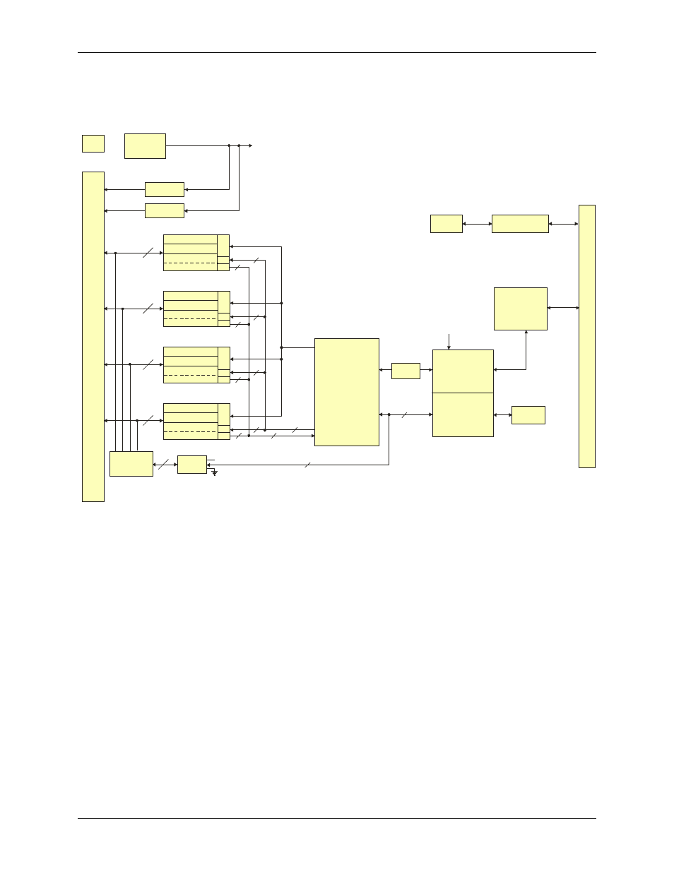
Functional block diagram
PCIe-DIO96H functions are illustrated in the block diagram shown here.
Figure 1. PCIe-DIO96H functional block diagram
GND
12
EEPROM
Switch
5V (VDD)
Boot
EEPROM
Interface
Decode/Status
Logic, Control,
1
0
0
-p
in
I
/O
C
o
n
n
e
c
to
r
10 k
Pull Resistor
Network
W
FIRSTPORTA
FIRSTPORTB
C
o
n
tr
o
l
High Drive FIRSTPORT
FIRSTPORTCL
FIRSTPORTCH
In
Out
SECONDPORTA
SECONDPORT B
C
o
n
tr
o
l
High Drive SECONDPORT
SECONDPORT CL
SECONDPORT CH
In
Out
THIRDPORTA
THIRDPORTB
C
o
n
tr
o
l
High Drive THIRDPORT
THIRDPORTCL
THIRDPORTCH
In
Out
FOURTHPORTA
FOURTHPORTB
C
o
n
tr
o
l
High Drive FOURTHPORT
FOURTHPORTCL
FOURTHPORTCH
In
Out
5V Power
Molex
Connector
Fuse
Protection
Spare
Fuse
24
24
24
24
+5V
+5V
Bus
Control
8
8
8
8
8
8
8
8
8
96
BP4
BP3
BP2
BP1
BP(1:4)
PCI-to-Local
Bus
BADR2
+
BADR3
Bus
Timing
LAD(0:7)
8
P
C
I
E
x
p
re
s
s
E
d
g
e
C
o
n
n
e
c
to
r
x1 Link
PCIe-to-PCI
Bridge
PCI Bus
3.3V
3.3V
1.5V
Regulator
3.3V, 32-bit, 33 MHz
Fuse
Protection
To +5V components
(Note: Outputs to CPLD
are 3.3V with 5V inputs)
+5V (VDD)
Local
Address
&
Data Bus
5V Detect
Software Sensing
Note: Port CL and CH
are tied together on
the pull resistors.
3.3V Board Power
Complex,
Programmable
Logic Device
(CPLD)
8