Functional details, Pci-dio24/lp block diagram, Chapter 3 – Measurement Computing PCI-DIO24/LP User Manual
Page 11
11
Chapter 3
Functional Details
The PCI-DIO24/LP board features the following:
82C55 digital I/O chip interfaced to the PCI bus. The I/O pins of an 82C55 are bi-directional CMOS TTL
level.
24-bits of digital I/O
68-pin I/O connector
The 82C55 provides the 24-bit digital I/O channels into three eight-bit ports labeled
Port A
,
Port B
and
Port C
.
Port C is further divided into two four-bit ports—PORTCL and PORTCH. You can program each port for input
or output.
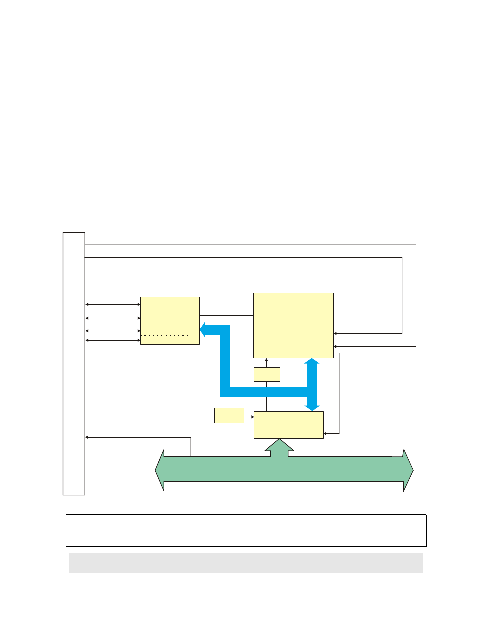
PCI-DIO24/LP block diagram
PCI-DIO24/LP functions are illustrated in the block diagram shown here.
PCI
CONTROLLER
BADR1
Boot
EEPROM
Control
Registers
Decode/Status
Bus
Timing
CONTROLLER FPGA and LOGIC
LOCAL BUS
PCI BUS (5V/3.3V, Universal 32-Bit, 33MHz)
CONTROL
BUS
PORT A
C
o
n
tr
o
l
PORT A (7:0)
82C55
Interrupt
Control
+5V
IRQ_INPUT
BADR2
Interrupt
IRQ_ENABLE
6
8
-P
in
I
/O
C
o
n
n
e
c
to
r
IRQ_INPUT
IRQ_ENABLE
PORT B (7:0)
PORT CH (3:0)
PORT B
PORT CH
PORT CL
PORT CL (3:0)
Figure 2. PCI-DIO24/LP functional block diagram
For more information on digital signal connections
For general information about digital signal connections and digital I/O techniques, refer to the Guide to Signal
Connections (available on our web sit
Caution! Do not connect high current/voltage devices directly to the PCI-DIO24/LP or you may damage the
board.