Functional details, Pci-dio24h block diagram, Dio signals – Measurement Computing PCI-DIO24H User Manual
Page 12: Chapter 3
12
Chapter 3
Functional Details
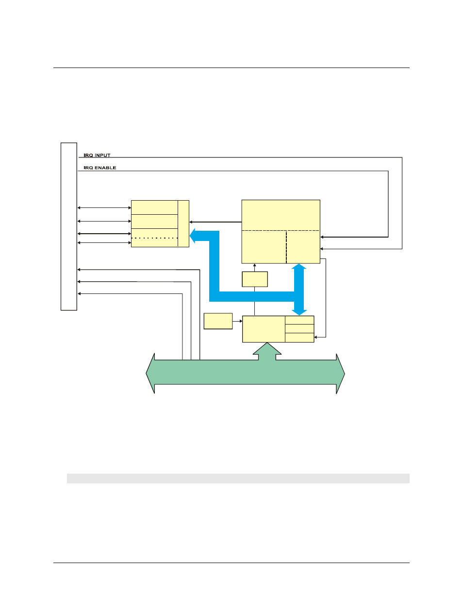
PCI-DIO24H Block diagram
PCI-DIO24H functions are illustrated in the block diagram shown here.
PCI
Controller
BADR1
Boot
EEPROM
Control
Registers
Decode/Status
Bus
Timing
Controller FPGA and logic
Local Bus
PCI BUS (5V, 32-bit, 33 MHZ)
Control
Bus
Interrupt
Control
+5V
+12V
-12V
BADR2
Interrupt
PORT A
C
o
n
tr
o
l
PORT A (7:0)
High Drive
82C55 Mode 0 Emulation
PORT B (7:0)
PORT CH (3:0)
PORT B
PORT CH
PORT CL
PORT CL (3:0)
IRQ INPUT
IRQ ENABLE
3
7
-P
in
I
/O
C
o
n
n
e
c
to
r
Figure 4. Functional block diagram
DIO signals
The PCI-DIO24H signals are buffered (high output drive) TTL. Voltages and currents associated with external
devices are usually far greater than can be supplied from a PCI-DIO24H.
Caution! Direct connections to high-current/high voltage devices will damage the board.
The emulated 82C55 mode 0 circuit initializes all ports as inputs on power-up and reset. The state of the digital
I/O lines is not defined as either logic high or logic low when in input mode. Input devices connected to the
PCI-DIO24 board may detect either a high or a low and therefore may be turned off or on at power-up.