0 data registers – Measurement Computing PC104-DI48 User Manual
Page 10
5.0 DATA REGISTERS
Each PC104-DI48 is composed of parallel input chips. Each address has one input
buffer that senses eight input pins. The ports are arranged in sets of three, with an
intervening N/A (not used) address area. This scheme allows compatibility with
software written to control 82C55 based boards when the 82C55 is used as all inputs.
(On those boards every fourth address contains a control register.)
The first address, or BASE ADDRESS, is determined by setting the base address
switches on the board. To read data from an input register, a byte is read representing
the status of all eight digital input lines. The individual bits are decoded as a (0) or a
(1). Data read from registers must be analyzed to determine which bits are on or off.
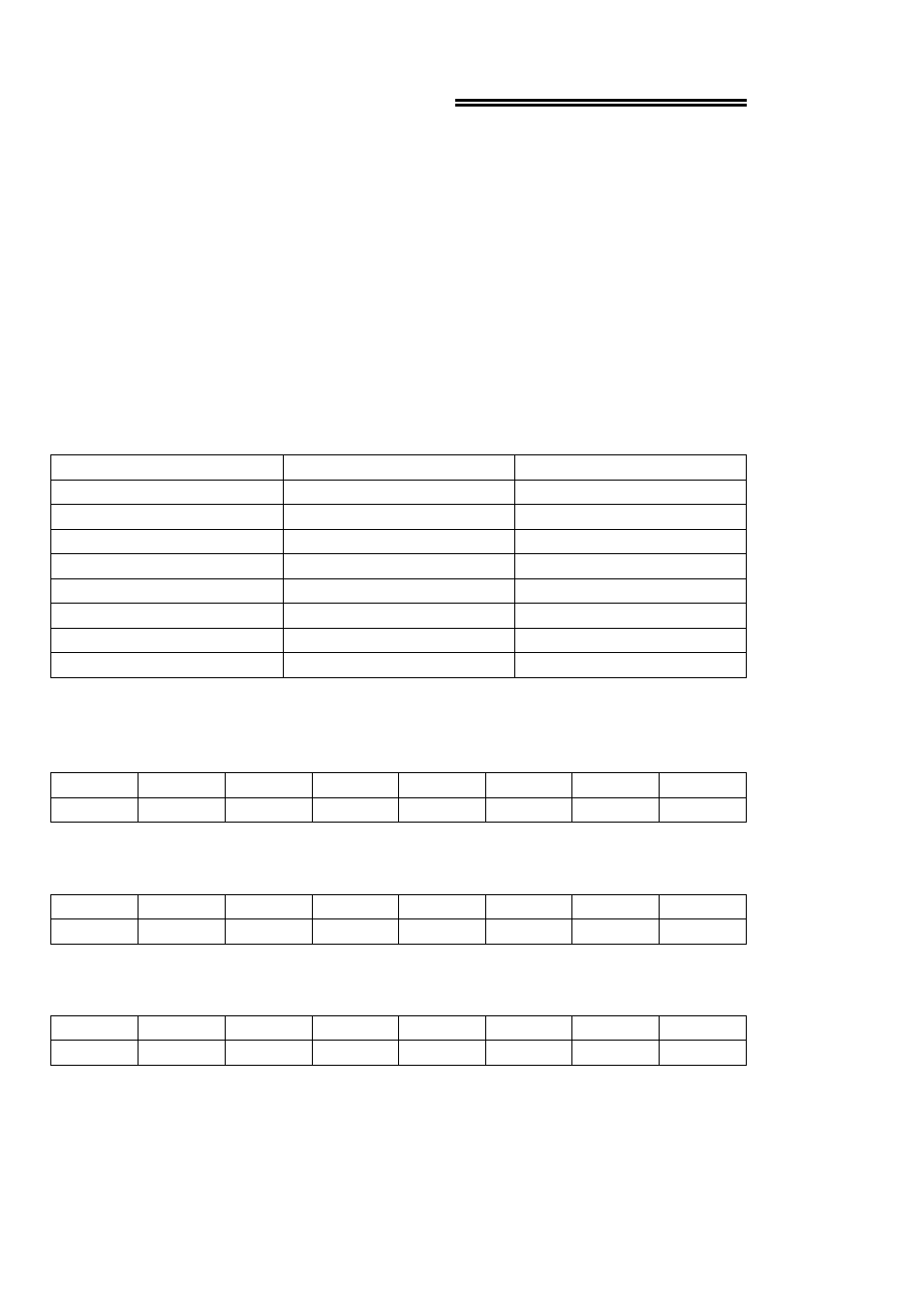
The registers and their function are listed on the following table. Each register has
eight bits of data.
None
BASE + 7
None
Port 2C Data
BASE + 6
None
Port 2B Data
BASE + 5
None
Port 2A Data
BASE + 4
None
BASE + 3
None
Port 1C Data
BASE + 2
None
Port 1B Data
BASE + 1
None
Port 1A Data
BASE + 0
WRITE FUNCTION
READ FUNCTION
ADDRESS
PORTS 1A and 2A DATA
BASE ADDRESS + 0, and +4
A0
A1
A2
A3
A4
A5
A6
A7
0
1
2
3
4
5
6
7
PORTS 1B and 2B DATA
BASE ADDRESS + 1, and +5
B0
B1
B2
B3
B4
B5
B6
B7
0
1
2
3
4
5
6
7
PORTS 1C and 2C DATA
BASE ADDRESS + 2, and +6
C0
C1
C2
C3
C4
C5
C6
C7
0
1
2
3
4
5
6
7
6