Functional details, Cio-dda06 block diagram, Signal connections – Measurement Computing CIO-DDA06 User Manual
Page 16: Chapter 4
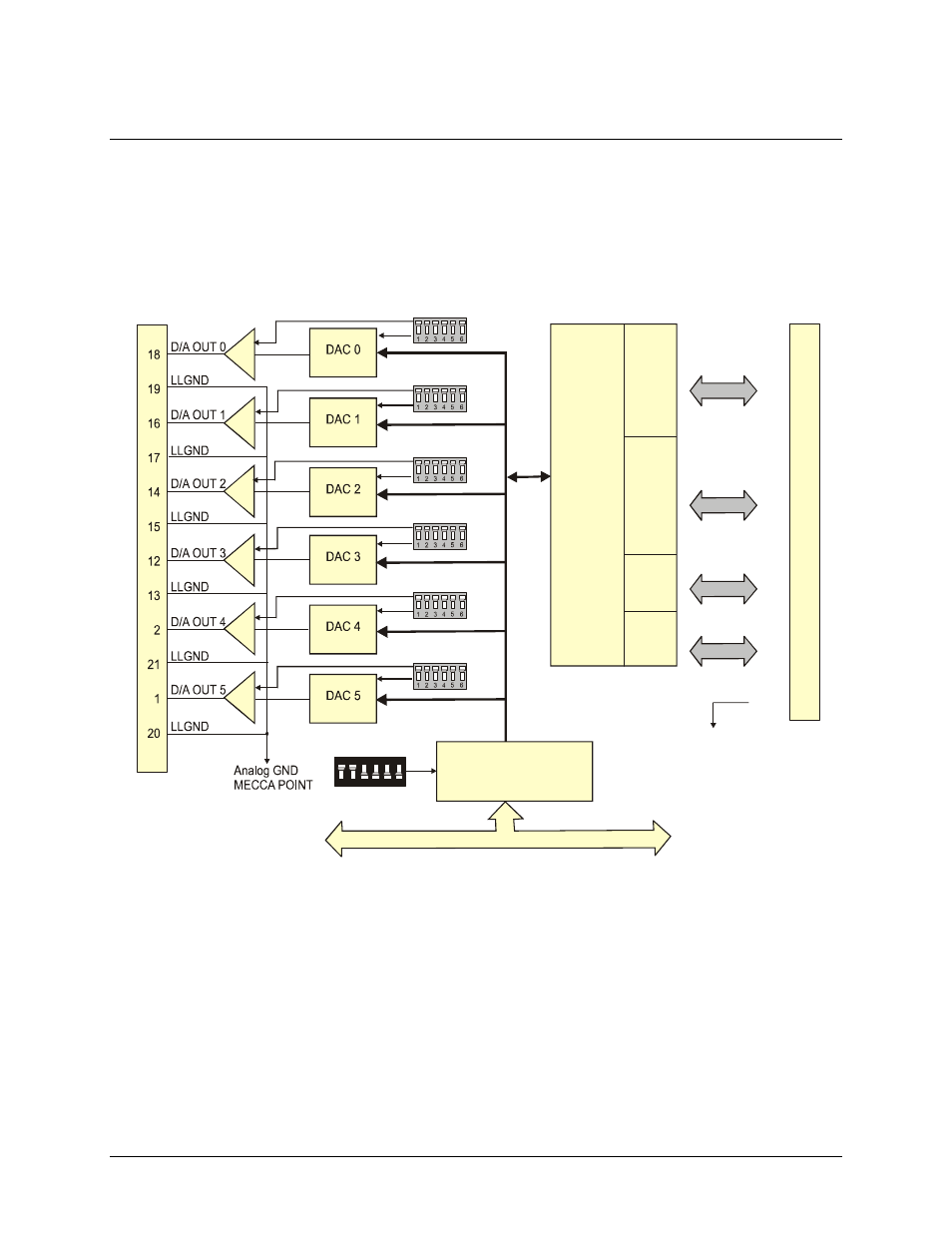
Chapter 4
Functional Details
CIO-DDA06 block diagram
CIO-DDA06 functions are illustrated in the block diagram shown here.
Data
Path
and
Control
8255
Digital I/O
9 8 7 6 5 4
ADDRESS
FI
RS
T
P
O
R
TA
F
IR
S
TP
O
R
TB
FIRSTPORTA Bit 0
Bit 1
Bit 2
Bit 3
Bit 4
Bit 5
Bit 6
Bit 7
FIRSTPORTB Bit 0
Bit 1
Bit 2
Bit 3
Bit 4
Bit 5
Bit 6
Bit 7
FIRSTPORTC Bit 0
Bit 1
Bit 2
Bit 3
FIRSTPORTC Bit 4
Bit 5
Bit 6
Bit 7
DGND
P/O
37-pin D conn.
37
36
35
34
33
32
31
30
10
9
8
7
6
5
4
3
29
28
27
26
25
24
23
22
11
Note: Digital I/O
pin assignments are
the same as for
the CIO-DIO24
ISA Bus
Address Decode
Bus Interface
Buffers and Transceivers
OP07
AD7237
AD7237
AD7237
AD7237
AD7237
AD7237
Gain switch
Gain switch
Gain switch
Gain switch
Gain switch
Gain switch
P/O
37-pin D conn.
OP07
OP07
OP07
OP07
OP07
FI
R
S
T
P
O
RT
C
LO
FI
R
S
T
P
O
RTC
HI
Signal connections
The CIO-DDA06 outputs are individually buffered through an OP07 operational amplifier (OP-AMP). The
OP07s are socketed so that if one fails it can be replaced in the field. The OP07 for each channel is located just
below the calibration potentiometers for that channel.
At the full rated output swing of ±10 V, each channel is capable of sinking or sourcing ±5 mA. A load of 2 KΩ
can be connected to each channel. As the load resistance rises from 2 K up to 10 MΩ or more, the output load
on the DAC decreases. Any load resistance greater than 2 k is acceptable.
16