Cio-dda06/16 block diagram, Data path and control – Measurement Computing CIO-DDA06/16 User Manual
Page 7
CIO-DDA06/16 User's Guide
Introducing the CIO-DDA06/16
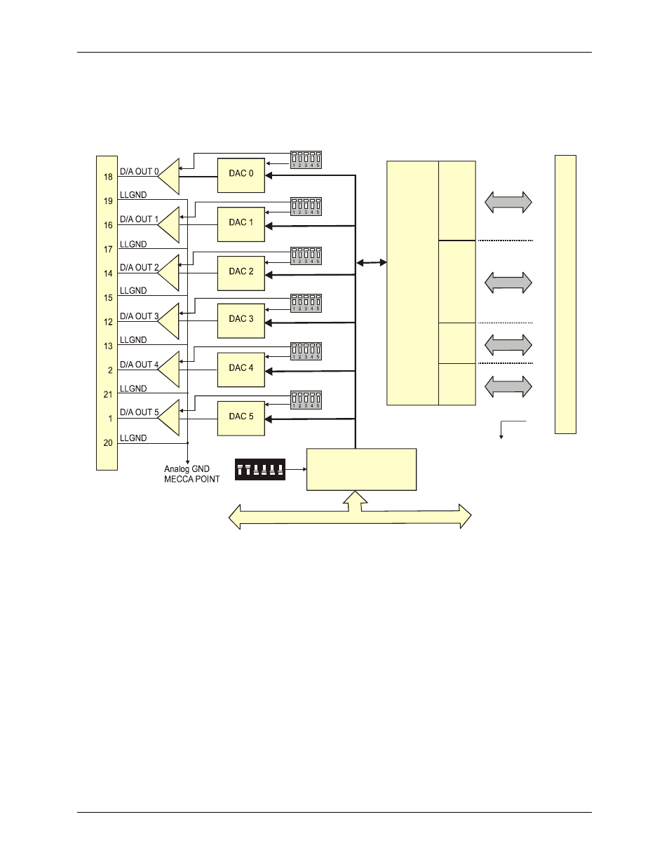
CIO-DDA06/16 block diagram
CIO-DDA06/16 functions are illustrated in the block diagram shown here.
8255
Digital I/O
9 8 7 6 5 4
ADDRESS
FIRSTPORTA Bit 0
Bit 1
Bit 2
Bit 3
Bit 4
Bit 5
Bit 6
Bit 7
FIRSTPORTB Bit 0
Bit 1
Bit 2
Bit 3
Bit 4
Bit 5
Bit 6
Bit 7
FIRSTPORTC Bit 0
Bit 1
Bit 2
Bit 3
FIRSTPORTC Bit 4
Bit 5
Bit 6
Bit 7
DGND
P/O
37-pin D conn.
37
36
35
34
33
32
31
30
10
9
8
7
6
5
4
3
29
28
27
26
25
24
23
22
11
Note: Digital I/O
pin assignments are
the same as for
the PCI-DIO24
ISA Bus
Address Decode
Bus Interface
Buffers and Transceivers
OP27
AD7237
AD660BN
Gain switch
P/O
37-pin D conn.
OP27
OP27
OP27
OP27
OP27
Data
Path
and
Control
FI
R
S
TP
O
R
T
A
FI
R
S
TP
OR
TB
F
IRS
T
POR
T
C
LO
FIRS
T
PO
R
T
C
HI
Gain switch
Gain switch
Gain switch
Gain switch
Gain switch
AD660BN
AD660BN
AD660BN
AD660BN
Figure 1. Functional block diagram
- ACC-300 (7 pages)
- AI-EXP32 (20 pages)
- AI-EXP48 (19 pages)
- BTH-1208LS (30 pages)
- 6K-ERB08 (32 pages)
- BTH-1208LS Quick Start (4 pages)
- 6K-SSR-RACK08 (33 pages)
- BTH-1208LS-OEM (27 pages)
- CB-COM-Digital (68 pages)
- CB-7018 (68 pages)
- CB-7000 Utilities (44 pages)
- CB-7080D (74 pages)
- CB-COM-7033 (44 pages)
- CB-COM-7017 (72 pages)
- CB-COM-7024 (76 pages)
- CB-NAP-7000P (36 pages)
- CIO-DAC02/16 (16 pages)
- CIO-DAC02 (18 pages)
- CB-NAP-7000D (56 pages)
- CIO-DAC16-I (16 pages)
- CIO-DAC16/16 (20 pages)
- CIO-DAS08 (21 pages)
- CIO-DAC16 (20 pages)
- CIO-DAS08/JR (16 pages)
- CIO-DAS08/JR/16 (14 pages)
- CIO-DAS08/JR-AO (16 pages)
- CIO-DAS08-AOM (32 pages)
- CIO-DAS08-PGM (28 pages)
- CIO-DAS16/330 (34 pages)
- CIO-DAS48-I (17 pages)
- CIO-DAS16/M1 (38 pages)
- CIO-DAS48-PGA (18 pages)
- CIO-DAS800 (20 pages)
- CIO-DAS802/16 (22 pages)
- CIO-DAS6402/16 (40 pages)
- CIO-DAS-TEMP (20 pages)
- CIO-DDA06/JR (17 pages)
- CIO-DIO24H (20 pages)
- CIO-DIO24/CTR3 (21 pages)
- CIO-DI192 (24 pages)
- CIO-DDA06 (21 pages)
- CIO-DIO48 (19 pages)
- CIO-DO192H (16 pages)
- CIO-DIO192 (20 pages)