Technical specifications – Delta Electronics Q48DC User Manual
Page 2

DS_Q48DC12003_03112008
2
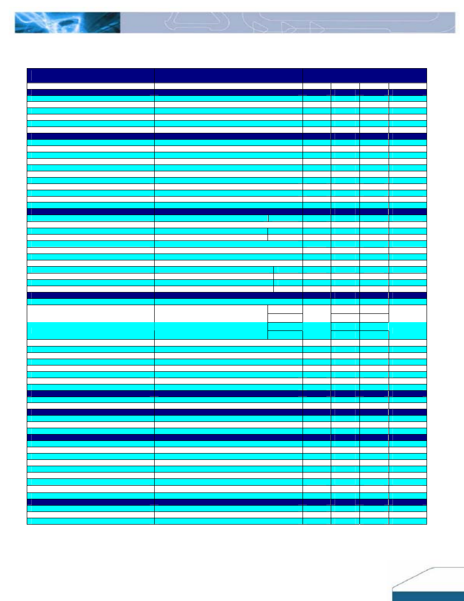
TECHNICAL SPECIFICATIONS
(T
A
=25°C, airflow rate=300 LFM, V
in
=48Vdc, nominal Vout unless otherwise noted.)
PARAMETER
NOTES and CONDITIONS
Q48DC12003NR A
Min. Typ. Max. Units
ABSOLUTE MAXIMUM RATINGS
Input Voltage
Continuous
80
Vdc
Transient
100ms
100
Vdc
Operating Temperature
Refer to Figure 20 for measuring point
-40
124
°C
Storage Temperature
-55
125
°C
Input/Output Isolation Voltage
2250
Vdc
INPUT CHARACTERISTICS
Operating Input Voltage
36
48
75
Vdc
Input Under-Voltage Lockout
Turn-On Voltage Threshold
32
33.5
35
Vdc
Turn-Off Voltage Threshold
29
30.5
32
Vdc
Lockout Hysteresis Voltage
2
3
4
Vdc
Maximum Input Current
100% Load, 36Vin
2.4
A
No-Load Input Current
50
mA
Off Converter Input Current
10
mA
Inrush Current(I
2
t)
1
A
2
s
Input Reflected-Ripple Current
P-P thru 12µH inductor, 5Hz to 20MHz
20
mA
Input Voltage Ripple Rejection
120Hz
66
dB
OUTPUT CHARACTERISTICS
Output Voltage Set Point
Vin=48V, lo=lo. Max, Tc=25℃
Vout 1,2
±
11.98
±
12.10
±
12.22
V
Output Voltage Regulation
Over Load
lo1=lo2=lo, min to lo, max
Vout 1,2
±
20
±
180
mV
Over Line
Vin=36V to 75V,Io1=Io2=full load
Vout 1,2
±
20
±
120
mV
Cross Regulation
| Io1-Io2| <20% Io,max
±
360
mV
Over Temperature
Tc=-40℃ to 129℃, Io1=Io2= Io, min to Io, max
±
120
mV
Total Output Voltage Range
Over all load, line and temperature
±
11.74
±
12.46
V
Output Voltage Ripple and Noise
5Hz to 20MHz bandwidth
Peak-to-Peak
Io1, Io2 Full Load, 1µF ceramic, 10µFtantalum
Vout 1, 2
40
80
mV
RMS
Io1, Io2 Full Load, 1µF ceramic, 10µF tantalum
Vout 1, 2
10
30
mV
Operating Output Current Range
Vout 1, 2
0
2.7
A
Output DC Current-Limit Inception
Iout 1+ lout 2
7.1
9
A
DYNAMIC CHARACTERISTICS
Output Voltage Current Transient
48V, 10µF Tan & 1µF Ceramic load cap, 0.1A/µs
Vout 1
400
600
Positive Step Change in Output Current
Iout1 or Iout2 from50% Io, max
to 75% Io, max
Vout 2
400 600
mV
Vout 1
400
600
Negative Step Change in Output Current
Iout2 or Iout1 from 75% Io,max
to 50% Io, max
Vout 2
400
600
mV
Cross dynamic
±
120
±
360
mV
Settling Time (within 1% Vout nominal)
100
us
Turn-On Transient
Delay Time, From On/Off Control
2
ms
Delay Time, From Input
2
ms
Start-up Time, From On/Off Control
20
30
ms
Start-up Time, From Input
20
30
ms
Maximum Output Capacitance
Full load; 5% overshoot of Vout at startup
5000
µF
EFFICIENCY
100% Load
Iout1, Iout2 full load
88
%
60% Load
Iout1, Iout2 60% of full load
86.5
%
ISOLATION CHARACTERISTICS
Input to Output
<1 minute
2250
Vdc
Isolation Resistance
10
MΩ
Isolation Capacitance
1500
pF
FEATURE CHARACTERISTICS
Switching Frequency
330
kHz
ON/OFF Control, (Logic Low-Module ON)
Logic Low
Von/off at Ion/off=1.0mA
-0.7
1.8
V
Logic High
Von/off at Ion/off=0.0 µA
3.5
12
V
ON/OFF Current
Ion/off at Von/off=0.0V
1
mA
Leakage Current
Logic High, Von/off=15V
300
uA
Output Voltage Trim Range
Pout ≦ max rated power (65W)
-17
+5
%
Iout ≦ max 120% rated Iout
-25 -17 %
Output Over-Voltage Protection
Over full temp range; %of nominal Vout
124
130
150
%
GENERAL SPECIFICATIONS
MTBF
Io=80% of Io, max; Ta=40°C
TBD
M hours
Weight
31
grams
Over-Temperature Shutdown
Refer to Figure 20 for measuring point
129
°C
