13 ecl interface -7, Ecl balanced (j8) -7, 2 ecl unbalanced data (j12) -7 – Comtech EF Data DD240XR Rev Е User Manual
Page 95: 3 ecl unbalanced clock (j13) -7
DD240XR High-Speed Digital Demodulator
Electrical Interfaces
MN-DD240XR – Rev. E
5-7
5.13 ECL Interface
5.13.1 ECL Balanced (J8)
The ECL Balanced Port (J8) is a female 9-Pin D-Sub Connector. Refer to Table 5-7 for pinouts.
5.13.2 ECL Unbalanced Data (J12)
The ECL Unbalanced Data Interface is a Female BNC Connector.
5.13.3 ECL Unbalanced Clock (J13)
The ECL Unbalanced Clock Interface is a Female BNC Connector.
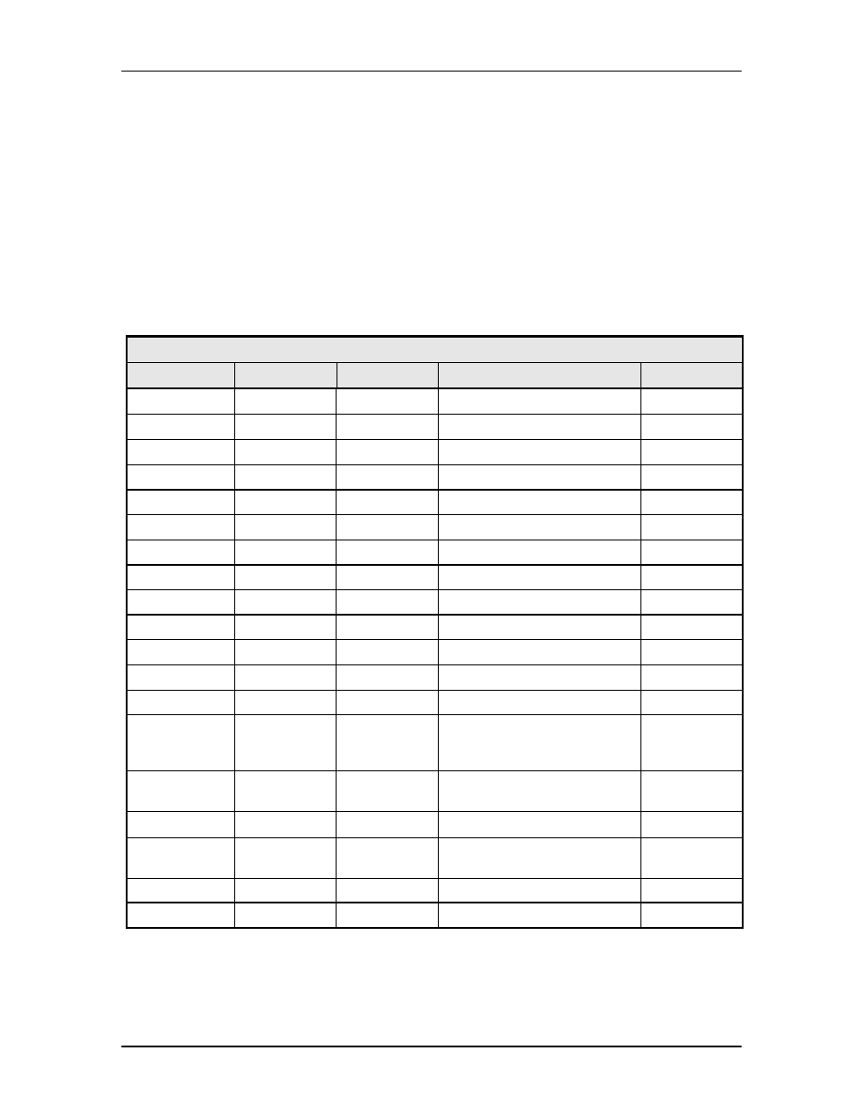
Table 5-6. J9 – HSSI (High-Speed Serial Interface) 50-Pin Connector
Pin No. (+)
Pin No. (–)
Signal Name
Description
Direction
1
26
SG
Signal Ground
-
2
27
RT
Receive Timing
Output
3
28
CA
DCE Available
Output
4
29
RD
Receive Data
Output
5
30
LC
Not Used
6
31
ST
Send Timing
N/A
7
32
SG
Signal Ground
-
8
33
TA
DTE Available
N/A
9
34
TT
Terminal Timing
N/A
10
35
LA
Loop back Circuit A
Not Used
11
36
SD
Send Data
N/A
12
37
LB
Loop back Circuit B
Not Used
13
38
SG
Signal Ground
-
15
40
EB CLK
External Bal. Clock
Used as EXT
BAL CLK
Input
14, 16 - 18
39, 41 – 43
4 Ancillary to
DCE
Input
19
44
SG
Signal Ground
-
20 - 22
45 - 47
3 Ancillary
from DCE
Output
24
49
TM
Output
25
50
Not Used