Preliminary technical specifications – Delta Electronics DNQ12 User Manual
Page 2
DS_DNQ12SIP25_07172008
2
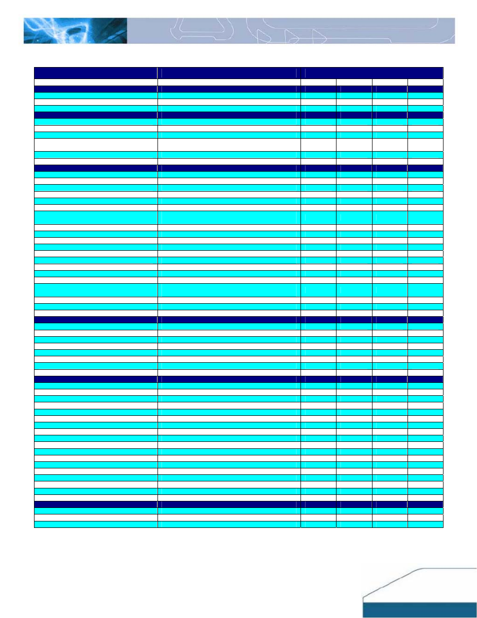
PRELIMINARY TECHNICAL SPECIFICATIONS
T
A
= 25°C, airflow rate = 300 LFM, V
in
= 10Vdc and 14Vdc, and nominal Vout unless otherwise noted.
PARAMETER
NOTES and CONDITIONS
DNQ12S0A0R25 (Standard)
Min.
Typ.
Max.
Units
ABSOLUTE MAXIMUM RATINGS
Input Voltage (Continuous)
-0.3
14
Vdc
Operating Temperature
Refer to figure 24 for measuring point
-40
125
°C
Storage Temperature
-55
125
°C
INPUT CHARACTERISTICS
Operating Input Voltage
10.0
12.0
14.0
Vdc
Maximum Input Current
Vin=10.0 to 14.0, Vo,set=5Vdc, Io=Io,max
14
Adc
Inrush Transient
1
A
2
s
Input Reflected Ripple Current (5Hz to 20MHz)
1µH source impedance; Vin,min to Vin,max, Io=Io,max ;
See Test configuration section
60
mAp-p
Input Ripple Rejection (120Hz)
50
dB
Recommended Input Fuse
See Safety Considerations section
30
A
OUTPUT CHARACTERISTICS
Output Voltage Set-point
Vin=Vin,min, Io=Io,max, T
A
=25°C
-1.2
+1.2
% Vo,set
Output Voltage Adjustable Range
Selected by an external resistor
0.7887
5.5
Vdc
Output Voltage Regulation
Over Line
Vin=Vin,min to Vin,max
0.01
0.1
% Vo,set
Over Load
Io=Io,min to Io,max
0.1
0.25
% Vo,set
Over Temperature
T
A
= T
A, min
to T
A, max
0.5
1.6
%
Vo,set
Total Output Voltage Range
Over all operating input voltage, resistive load, and
temperature conditions until end of life
-3.0
+3.0
% Vo,set
Output Voltage Ripple and Noise
Cout=10µF tantalum//1µF ceramic capacitors
RMS (5Hz to 20MHz bandwidth)
Vin=Vin,typ, Io=Io,min to Io,max
5
15
mVrms
Peak-to-Peak (5Hz to 20MHz bandwidth)
Vin=Vin,typ, Io=Io,min to Io,max
15
50
mVp-p
External Capacitance
ESR ≧1mΩ
1000
µF
ESR ≧10mΩ at Vo,set=5Vdc
5,000
µF
ESR ≧10mΩ at Vo,set below 3.3Vdc
10,000
µF
Output Current
0
25
Adc
Output Current Limit Inception (Hiccup Mode)
150
200
% Io
Output Short-Circuit Current (Hiccup Mode)
Vo ≦ 250mV
1
Adc
Dynamic Load Response
dIo/dt=5A/µs, Vin=Vin,typ, T
A
=25°C,
Cout=10µF tantalum//1µF ceramic capacitors
Positive Step Change in Output Current
Load change from 50% to 100% of Io,max
150
mV
Negative Step Change in Output Current
Load change from 100% to 50% of Io,max
150
mV
Settling Time (Vo<10%peak deviation)
25
µs
EFFICIENCY
Vo,set =0.8V
Vin=Vin,typ, Io=Io,max, T
A
=25°C
79.0
%
Vo,set =1.2V
Vin=Vin,typ, Io=Io,max, T
A
=25°C
84.7
%
Vo,set =1.5V
Vin=Vin,typ, Io=Io,max, T
A
=25°C
87.3
%
Vo,set =1.8V
Vin=Vin,typ, Io=Io,max, T
A
=25°C
88.9
%
Vo,set =2.0V
Vin=Vin,typ, Io=Io,max, T
A
=25°C
89.7
%
Vo,set =2.5V
Vin=Vin,typ, Io=Io,max, T
A
=25°C
91.4
%
Vo,set =3.3V
Vin=Vin,typ, Io=Io,max, T
A
=25°C
93.1
%
Vo,set =5.0V
Vin=Vin,typ, Io=Io,max, T
A
=25°C
95.1
%
FEATURE CHARACTERISTICS
Switching Frequency
500
kHz
SEQ/ENA
Signal
Interface
Logic High (SEQ/ENA pin open - Module Off)
SEQ/ENA Voltage
Vin=Vin,min to Vin,max
3.5
14
V
SEQ/ENA Current
Vin=Vin,min to Vin,max
0.5
2.33
mA
Logic Low (Module ON)
SEQ/ENA Voltage
Vin=Vin,min to Vin,max
1.2
V
SEQ/ENA Current
Vin=Vin,min to Vin,max
200
µA
Turn-On Transient
Vin=Vin,typ, Io=Io,max
Turn-On delay Time, From remote On/Off
From V
SEQ/ENA
=1.2V to Vo=10% of Vo,set
1
ms
Turn-On delay Time, From Input
From Vin= Vin,min to Vo=10% of Vo,set
1
ms
Turn-On rise Time
Time for Vo to rise from 10% to 90% of Vo,set
5
ms
Output Voltage Overshoot - Startup
Io=80% of Io,max, Vin=12Vdc, T
A
=25℃
0.1
0.5
% Vo,set
Output Overvoltage Protection (Latching)
5.7
6.0
6.3
V
Input Undervoltage Lockout
Turn-on Threshold
9.9
V
Turn-off Threshold
8.1
V
Remote Sense Range
0.5
V
GENERAL SPECIFICATIONS
MTBF
Io=80%Io, max, Ta=25℃
3.03
MHours
Weight
20
Grams
Over-Temperature Shutdown
Refer to Figure 24 for the measuring point
130
°C