1 overview, Block diagram, 1overview – ADLINK LEC-3517 User Manual
Page 5: Pin smarc connector, 1 block diagram, Texas instruments micro processor, Am3517 texas instruments

Overview
1
LEC-3517
1
Overview
This initial manual version presents a general overview of the LEC-3517 Computer-On-Module
(COM). The next version of this manual shall include more detailed information including user
interface descriptions, boot setup access and menu settings, memory map, interrupt channel
assignments, and I/O address map. After reviewing this document you should understand the
following features of the LEC-3517.
Functional Block Diagram
Major Component (IC) Locations and Descriptions
Connector Location and Description
Specifications
SMARC Interface Signal Definitions
NOTE: Please refer to BSP readme documents in the Quick Drive for BSP installation instruc-
tions.
1.1 Block Diagram
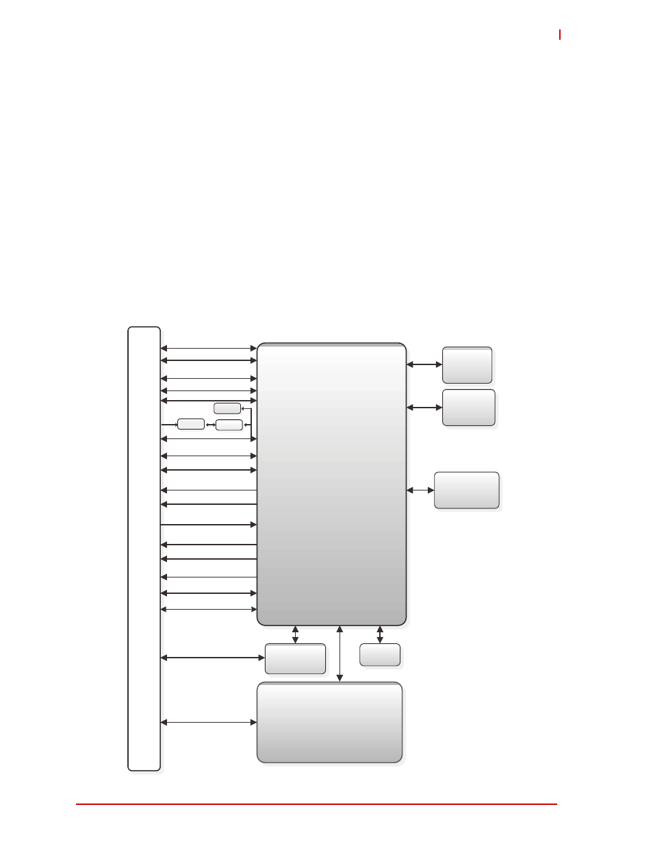
Figure 1-1 represents the component functions of the module.
Figure 1-1: Functional Block Diagram
314-pin SMARC Connector
Texas Instruments
Micro Processor
®
AM3517
Texas Instruments
®
PMIC
(Power Management IC)
TPS650732
Memory
1Gb DDR2
64x16
NAND
4Gb (8-bit)
Memory
1Gb DDR2
64x16
USB1 Host
USB0 Host/OTG
4x UART
(2x 4-pin, 2x 2-pin)
LCD 24-bit RGB
LAN PHY
SMSC LAN8710A-EZK
10/100 Mbps
Power
1x CAN
SPI0 / SPI1
I
2
S (3x)
I
2
C (3x)
GPIO (12x)
SDMMC (8-bit)
SDIO (4-bit)
10-pin JTAG
connector
Watchdog
Management
Camera (8-bit) +I
2
C
LCD Support + I
2
C
Boot Select (0,1,2)
Force Recovery
LEC_3517_Blk_Diag_a
EEPROM
Level
Shift
RTC
VRTC
