1 overview, Block diagram, 1overview – ADLINK LEC-iMX6 User Manual
Page 5: Pin smarc connector, 1 block diagram, Freescale imx6, Functional block diagram, Specifications, Boot up configuration

Overview
1
LEC-iMX6
1
Overview
This initial manual version presents a general overview of the LEC-iMX6. After reviewing this
document you should understand the following features of the LEC-iMX6.
Functional Block Diagram
Major Components (ICs) and Connectors (Locations and Descriptions)
Specifications
Boot Up Configuration
Interface Signal and Power Management Definitions
NOTE: Please refer to BSP readme documents in the Quick Drive for BSP installation instruc-
tions.
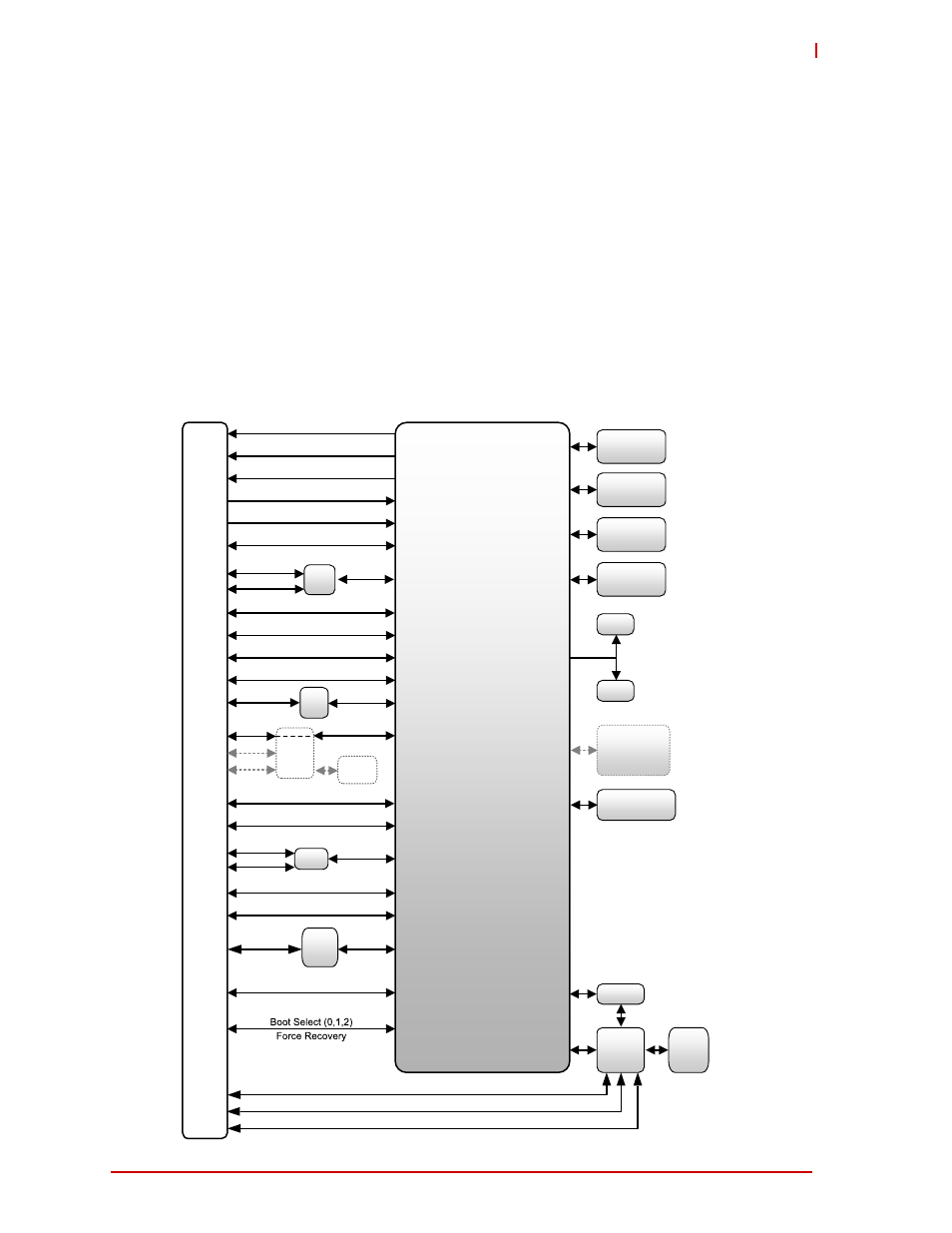
1.1 Block Diagram
Figure 1-1 represents the component functions of the module.
Figure 1-1: Functional Block Diagram
314-pin SMARC Connector
Freescale
iMX6
Memory
DDR3L
eMMC
(optional)
USB0 Host/OTG
LCD 24-bit RGB
eMMC/SDMMC (8-bit)
SDIO (4-bit)
40-pin Debug
Connector
PCAM (10-bit)
Memory
DDR3L
Memory
DDR3L
Memory
DDR3L
USB2 Host
USB1 Host
BMC
LM73
Thermal
Sensor
GbE
LAN
PHY
RGMII
SATA
1x I2C (option)
3x I2C
LVDS 24-bit (incl. DDC)
HDMI (Including DDC and CEC)
PCA
9535A
GPIO
12x GPIO
PCIe
switch
(option)
PCIe
PCIe
PCIe
PCIe
4x UARTS (2x 4, 2x 2)
2x CAN
MLB
SPDIF
MIPI CSI Camera, 2 lanes
MUX
I2S
SPI
SPI/I2S
1x SPI
SPI
Flash
(option)
RTC
Flash
Flash
1x SPI
1x I2C
USB
Hub
USB
Watchdog
LEC_iMX6_blk_diag_d
Power Management
