6 connectors and pin-outs, 1 carrier board signals, 2 connector and pinout compatibility – ADLINK Express-BASE User Manual
Page 12: 3 carrier board design, Carrier board signals, Connector and pinout compatibility, Carrier board design

Express-BASE User’s Manual
Page 12
C D
A B
6 Connectors and Pin-outs
6.1 Carrier Board Signals
6.2 Connector and Pinout Compatibility
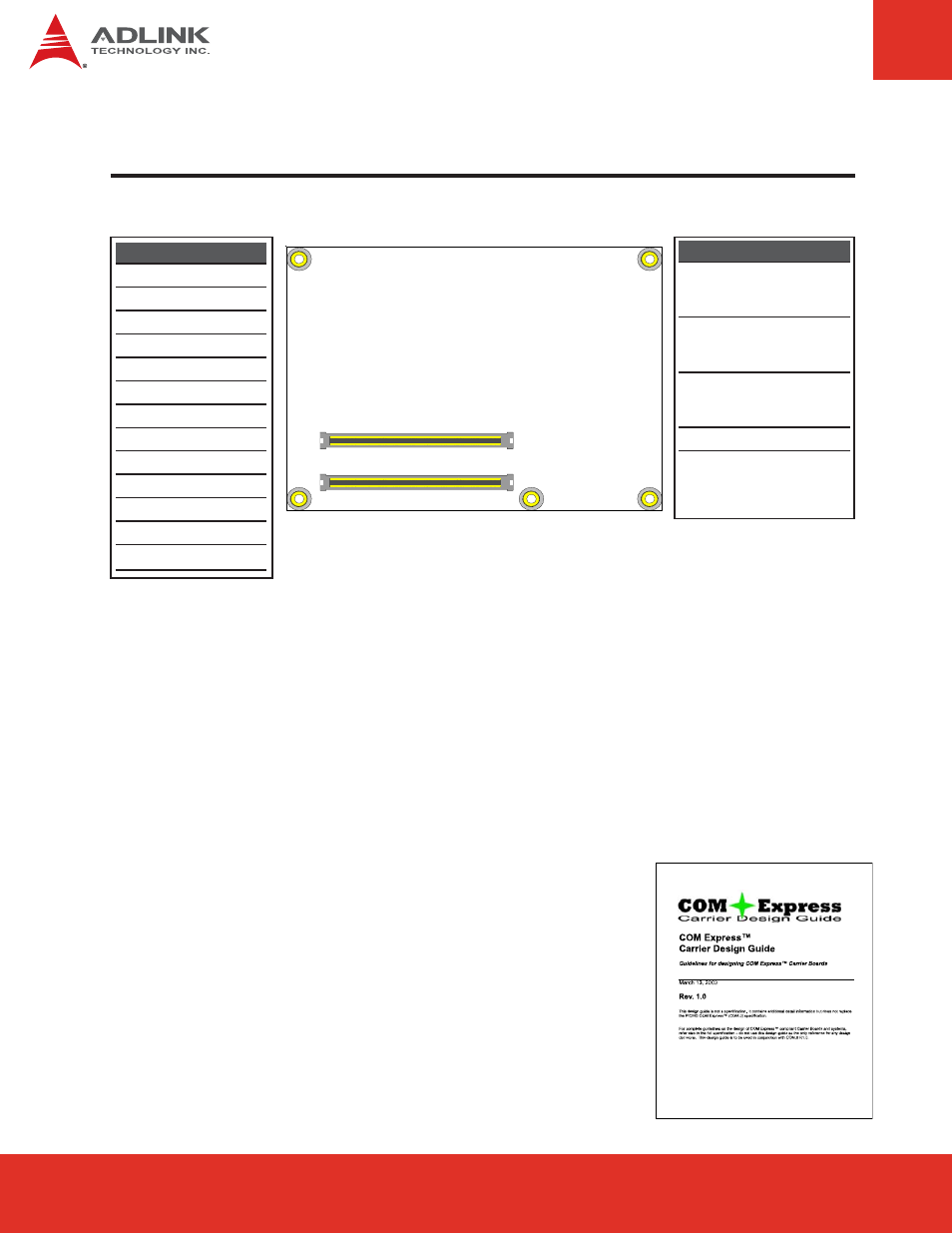
Connectors positions and pinouts comply with pinout and signal descriptions in the “PICMG®
COM.0 - COM Express Module Base specification, Revision 2”. This document includes:
description of pinouts, signal descriptions and mechanical characteristics of the COM Express
specification. The Express-BASE is compatible with COM Express modules in Basic and
Compact form factor, Type 2 pinout, COM.0 Rev. 1.0 and Rev. 2.0.
6.3 Carrier Board Design
The Express-BASE closely follows the PICMG COM Express™
Carrier Design Guide (CDG). Please note that the CDG gives
design advice, and contains unverified reference schematics. The
Express-BASE design and schematics are fully verified, and we
recommend that you follow them as a reference for your carrier
board design.
The CDG and Express-BASE Rev. D2 Schematics and
Mechanical files can be downloaded from the ADLINK
Express-BASE product webpage:
AB Connector
1 Gigabit Ethernet port
LPC interface
4 Serial ATA channels
High Definition Audio
8 USB 2.0 ports
6 PCI Express Lanes x1
Dual 24-bit LVDS channels
Analog VGA
TV-out ports (SDTV/HDTV)
8 GPIO pins
SMB and I
2
C bus
+12V primary power input
+5V standby and 3V
RTC
CD Connector
Parallel ATA, IDE port
alternate definition assigns this to
2 additional Gigabit Ethernet ports
32-bit PCI v2.3 bus
alternate definition assigns this to
10 additional PCI Express x1 lanes
PCI Express x16 for Graphics
these pins can also be assigned to
two SDVO extensions (multiplexed)
+12V primary power input
