ADLINK Express-IBE2 User Manual
Page 28
Page 28
Express-IBE2
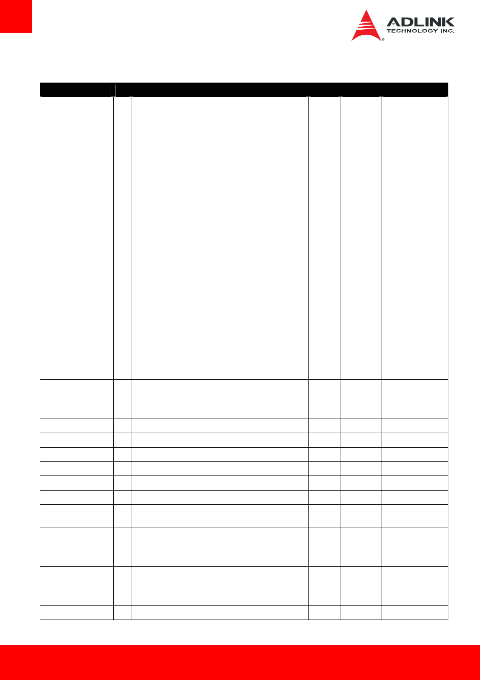
3.4.2. PCI
Signal
Pin Description
I/O
PU/PD
Comment
PCI_AD0
PCI_AD1
PCI_AD2
PCI_AD3
PCI_AD4
PCI_AD5
PCI_AD6
PCI_AD7
PCI_AD8
PCI_AD9
PCI_AD10
PCI_AD11
PCI_AD12
PCI_AD13
PCI_AD14
PCI_AD15
PCI_AD16
PCI_AD17
PCI_AD18
PCI_AD19
PCI_AD20
PCI_AD21
PCI_AD22
PCI_AD23
PCI_AD24
PCI_AD25
PCI_AD26
PCI_AD27
PCI_AD28
PCI_AD29
PCI_AD30
PCI_AD31
C24
D22
C25
D23
C26
D24
C27
D25
C28
D27
C29
D28
C30
D29
C32
D30
D37
C39
D38
C40
D39
C42
D40
C43
D42
C45
D43
C46
D44
C47
D45
C48
PCI bus multiplexed address and data lines
I/O 3.3V
PCI_C/BE0#
PCI_C/BE1#
PCI_C/BE2#
PCI_C/BE3#
D26
C33
C38
C44
PCI bus byte enable lines, active low.
I/O 3.3V
PCI_DEVSEL#
C36 PCI bus Device Select, active low.
I/O 3.3V
PU 8k2 3.3V
PCI_FRAME#
D36 PCI bus Frame control line, active low.
I/O 3.3V
PU 8k2 3.3V
PCI_IRDY#
C37 PCI bus Initiator Ready control line, active low.
I/O 3.3V
PU 8k2 3.3V
PCI_TRDY#
D35 PCI bus Target Ready control line, active low.
I/O 3.3V
PU 8k2 3.3V
PCI_STOP#
D34 PCI bus STOP control line, active low, driven by cycle initiator.
I/O 3.3V
PU 8k2 3.3V
PCI_PAR
D32 PCI bus parity
I/O 3.3V
PCI_PERR#
C34 Parity Error: an external PCI device drives PERR# when it
receives data containing a parity error.
I/O 3.3V
PU 8k2 3.3V
PCI_REQ0#
PCI_REQ1#
PCI_REQ2#
PCI_REQ3#
C22
C19
C17
D20
PCI bus master request input lines, active low.
I 3.3V
PU 8k2 3.3V
PCI_GNT0#
PCI_GNT1#
PCI_GNT2#
PCI_GNT3#
C20
C18
C16
D19
PCI bus master grant output lines, active low.
O 3.3V
PCI_RESET#
C23 PCI Reset output, active low.
O 3.3V