4 communication states, 5 wdt & bypass control logic, Communication states – ADLINK PMC-8246 User Manual
Page 17: Wdt & bypass control logic
Introduction
5
PMC-8246
1.4
Communication States
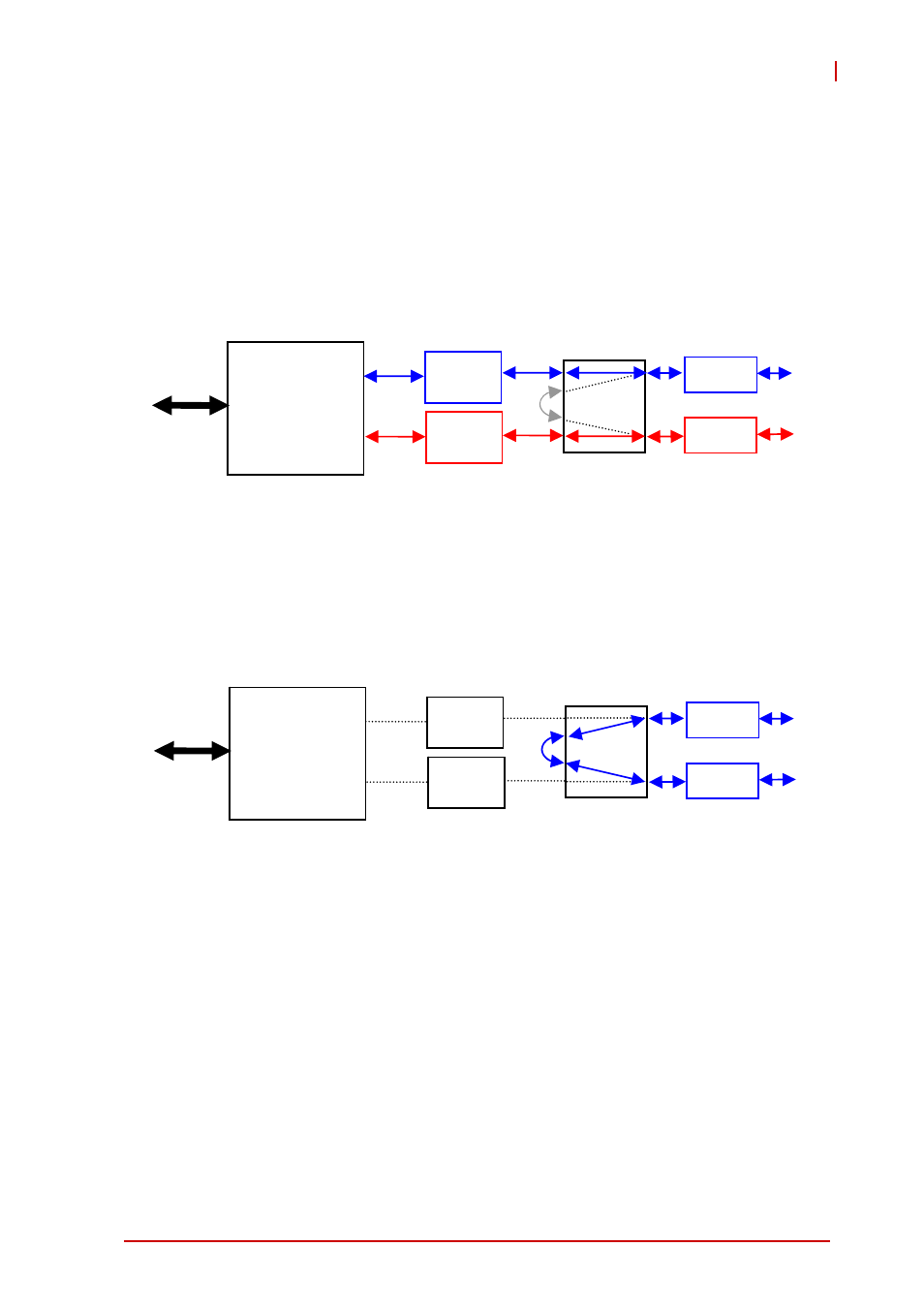
The following diagram illustrates the Normal State: where the two
GbE signals are straight-through connected to the GbE ports via
the transformers. The two GbE ports work independently as nor-
mal dual GbE ports.
Figure 1-1: Communication States: Normal
The following diagram shows the Bypass State: where the two
GbE signal are cross-over connected to each other so that the
Ethernet connection bypasses the computer or the network appli-
ance where this PMC module is installed in.
Figure 1-2: Communication States: Bypass
The relay array is driven by the relay divers which are controlled
by the watchdog timer and bypass control logic circuits.
1.5
WDT & Bypass Control Logic
The block diagram of the WDT and bypass control logic circuits is
as follows:
82546GB
Dual GbE
Trans-
former
Trans-
former
PCI-X
Bus
Relay Array
RJ-45
RJ-45
GbE #1
GbE #2
82546GB
Dual GbE
Trans-
former
Trans-
former
PCI-X
Bus
Relay Array
RJ-45
RJ-45
GbE #1
GbE #2