ADLINK ND-6018 User Manual
Page 29

Introduction
• 21
Note
(6)
: The maximum input voltage shall not exceed to ±30V with reference to
AGND otherwise, they may cause an unrecoverable harm to the hardware
component.
Note
(7)
: F/W version above C4.30 support K-type for 0~1370
°
C. Lower version
supports K-type for 0~1000
°
C.
Pin Definitions of ND-6018
Pin #
Signal Name Description
1
Vin5+
Differential positive input channel 5
2
Vin5-
Differential negative input channel 5
3
Vin6+
Single-ended voltage input channel 6
4
AGND
Analog signal ground of CH6 & 7
5
Vin7+
Single-ended voltage input channel 7
6
DEFAULT*
Initial state setting
7
(Y) DATA+
RS-485 series signal, positive
8
(G) DATA-
RS-485 series signal, negative
9
(R) +Vs
Power supply, +10V~+30V
10 (B)
GND Ground
11
Vin0+
Differential positive input channel 0
12
Vin0-
Differential negative input channel 0
13
Vin1+
Differential positive input channel 1
14
Vin1-
Differential negative input channel 1
15
Vin2+
Differential positive input channel 2
16
Vin2-
Differential negative input channel 2
17
Vin3+
Differential positive input channel 3
18
Vin3-
Differential negative input channel 3
19
Vin4+
Differential positive input channel 4
20
Vin4-
Differential negative input channel 4
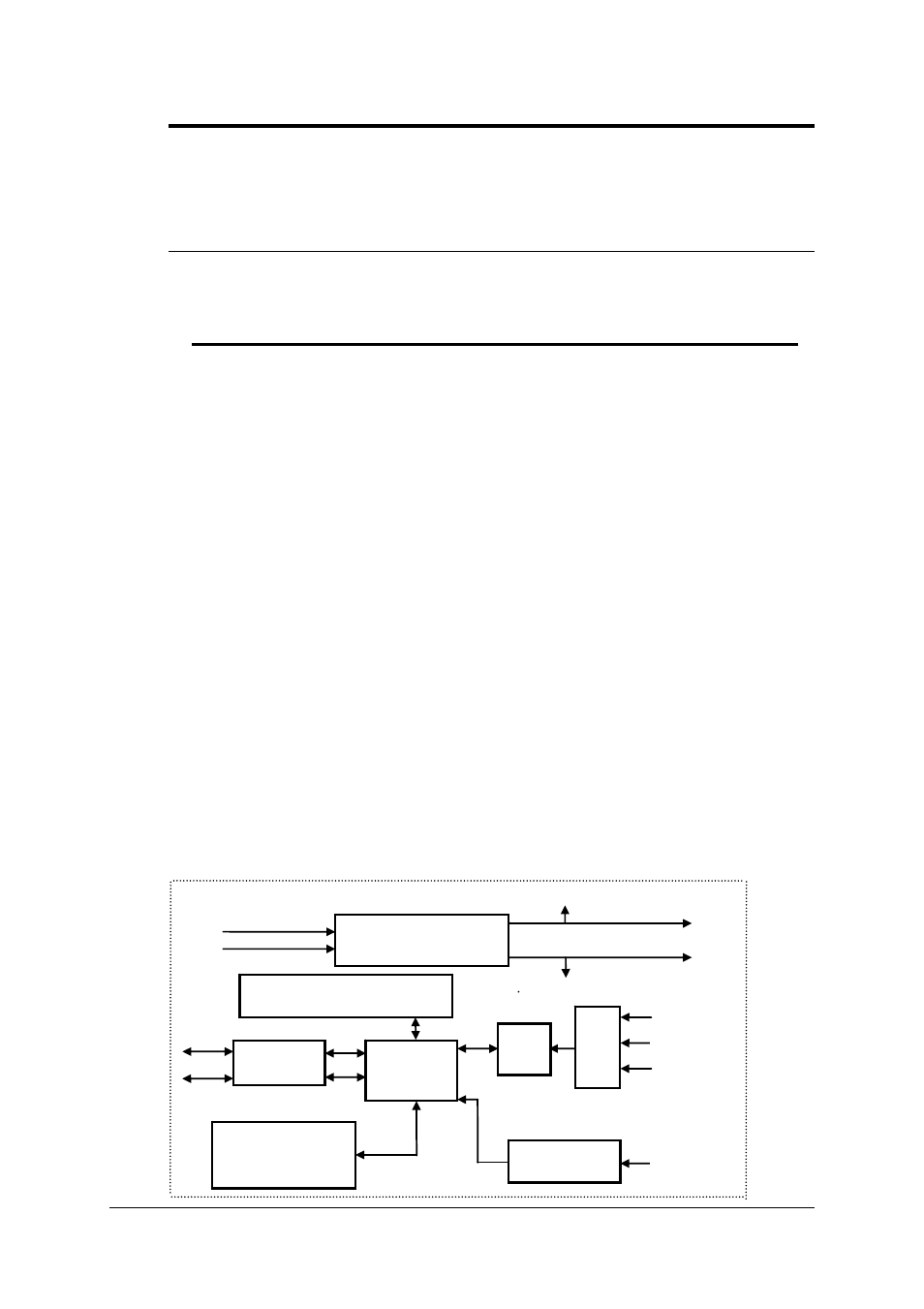
Functional Block Diagram of ND-6018
Power Input
+10V ~ +30V
+ 5V
Power
Regulator & Filter
Data+
Data -
GND
RS-485
Rec/Drv
Micro
Processor
EEPROM
Config Data
Safe Value
ADC
1-bit
Digital Input
8
Thermo-
couple
Input
channels
Default*
Pin
Mux
Watchdog/Power Failure
Supervisor
