3 analog output status register, 4 digital output register, 5 digital input register – ADLINK cPCI-6208V User Manual
Page 28

20
•
Registers
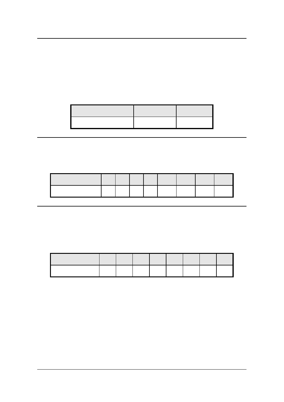
3.3 Analog Output Status Register
The DAC uses a series bus architecture hence it will take time for digital
value to be sent out. The data transfer rate for every DA data write takes
2.2
µ
s, therefore the software driver must wait 2.2
µ
s before sending any
other data to any analog output port. While the DA value is sending, the
Data_Send bit is ‘H’. The software driver should check this bit before
writing any data to the output port. This register is read only.
Offset Address
D16~D1
D0
0x00
X
Data_Send
3.4 Digital Output Register
D0~D3 is the digital output signal written to the output channels. D4~D7
are don’t cares.
Offset Address D7 D6 D5 D4
D3
D2
D1
D0
0x40
X
X
X
X
DO3 DO2 DO1 DO0
3.5 Digital Input Register
D4~D7 is digital input signal from CN1.
D0~D3 is read back signal from digital output channel.
Offset Address D7
D6
D5
D4
D3
D2
D1
D0
0x40
DI3 DI2 DI1 DI0 DO3 DO2 DO1 DO0
