3 operation, 1 functional layout, 2 signal sources – ADLINK USB-2401 User Manual
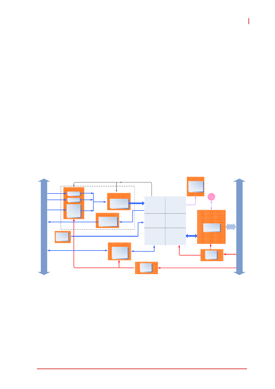
Page 37: 1 floating signal source, Functional layout, Signal sources, Floating signal source, Figure 3-1, Usb-2401 functional block diagram, 3operation

Operation
27
USB-2401
3
Operation
Operation of the USB-2401 is described here to assist in
configuration and programming of the module. Functions
described include A/D conversion, programmable function I/O,
and others
3.1
Functional Layout
The USB-2401 provides 4-channel 24-bit universal analog inputs
and supports seven input modes, including voltage input, current
input, thermocouple, RTD, full bridge, half bridge, and resistance
measurement. The four channels sample simultaneously, and
while each can be configured to a different input mode, all active
channels must be configured to the same sampling rate. In
addition, the USB-2401 also provides 6-channel programmable
digital I/O and can be configured to GPIO, GPTC, or PWM mode.
Figure 3-1: USB-2401 Functional Block Diagram
3.2
Signal Sources
3.2.1
Floating Signal Source
Not connected in any way to the existing ground system.
Devices with isolated output are floating signal sources, such as
optical isolator outputs, transformer outputs, and thermocouples.
40P CON
NEC
T
O
R
INTERFACE
ADLINK
FPGA Core
8051 Core
Function
Interface
AFI
Control signal
GPIO
GPTC
PWM
Functional I/O
24 Bit
Sigma-
delta ADC
ADC Front end
4DI , 2DO
DATA
DDR2 SDRAM
US
B 2.0 IN
TE
RFAC
E
Cypress
CY7C68013A
USB 2.0
High-Speed
24MHz XTAL
8051 Core 12/
24/48MHz
Digital I/O
Controller
AI Data and
Control
I2C
Interface
EEPROM
ADC
Calibration
Controller
Power
circuit
±4,±2.5V
USB BUS
+5V Supply
Data/
Control
Bridge-based
RTD
Resistor
Thermocouple
Mode
Power
circuit
3.3 2.5 1.2V
Supply
USB BUS
+5V Supply
3.3V Supply
3.3/2.5/1.2V
Voltage
Current
Calibration
data
AFI
Voltage (2.5V)
Current (0.5mA, 0.05mA)
Excitation Source
AIn+, AIn-
CIn+, CIn-
SCn+, SCn-
EXCn
n=0 ~3
CJC
(Cold Junction
Compensation)
