Absolute maximum ratings, Ww.nl ic, Com/adi – Analog Devices AD604 User Manual
Page 5: Ad604
Attention! The text in this document has been recognized automatically. To view the original document, you can use the "Original mode".
AD604
ABSOLUTE MAXIMUM RATINGS
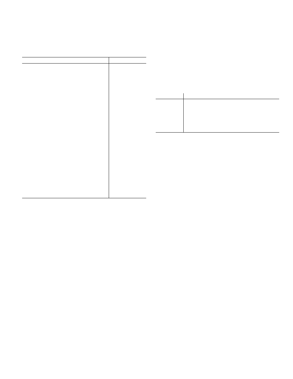
Table 2.
Rating
Supply Voltage ±Vs
Pin 17 to Pin 20 (with Pin 16, Pin 22 = 0 V)
Input Voltages
±6.5 V
Pin 1, Pin 2, Pin 11, Pin 12
VPOS/2 ± 2 V
continuous
Pin 4, Pin 9
±2 V
Pin 5, Pin 8
VPOS, VNEG
Pin 6, Pin 7, Pin 13, Pin 14, Pin 23, Pin 24
VPOS, 0 V
Internal Power Dissipation
PDIP (N)
2.2 W
SOIC (RW)
1.7 W
SSOP (RS)
1.1 W
Operating Temperature Range
-40°C to +85°C
Storage Temperature Range
-65°C to +150°C
Lead Temperature, Soldering 60 sec
300°C
AD604AN
105°C/W
AD604AR
73°C/W
AD604ARS
112°C/W
AD604AN
AD604A
^WW.nl IC
Stresses above those listed under Absolute Maximum Ratings
may cause permanent damage to the device. This is a stress
rating only; functional operation of the device at these or any
other conditions above those indicated in the operational
section of this specification is not implied. Exposure to absolute
maximum rating conditions for extended periods may affect
device reliability.
ESD CAUT ON
>
ESD (electrostatic discharge) sensitive device.
Charged devices and circuit boards can discharge
without
detection.
Aithough
this
product
features
patented or proprietary protection circuitry, damage
may occur on devices subjected to high energy ESD.
Therefore, proper ESD precautions should be taken to
avoid performance degradation or ioss of functionaiity.
.com/ADI
1
Pin 1, Pin 2, Pin 11 to Pin 14, Pin 23, and Pin 24 are part of a single-supply
circuit. The part is likely to suffer damage if any of these pins are accidentally
connected to VN.
2
When driven from an external low impedance source.
3
Using MIL-STD-883 test method G43-87 with a 1S (2-layer) test board.
Rev. E | Page 5 of 32