Applications information, Ad604 – Analog Devices AD604 User Manual
Page 18
Attention! The text in this document has been recognized automatically. To view the original document, you can use the "Original mode".
AD604
APPLICATIONS INFORMATION
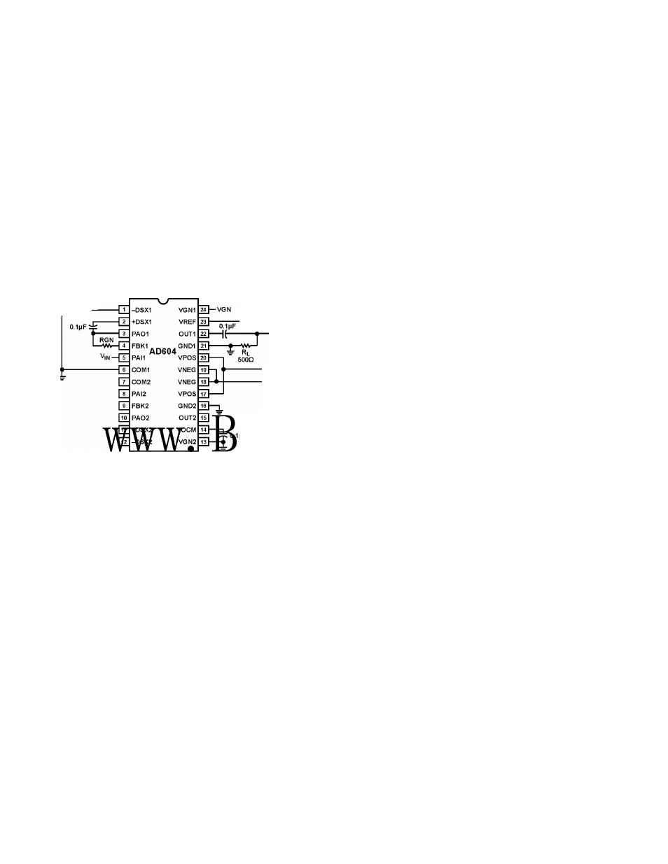
The basic circuit in Figure 43 shows the connections for one
channel of the AD604. The signal is applied at Pin 5. RGN is
normally 0, in which case the preamplifier is set to a gain of 5
(14 dB). When FBK1 is left open, the preamplifier is set to a
gain of 10 (20 dB), and the gain range shifts up by 6 dB. The ac
coupling capacitors before -DSX1 and +DSX1 should be selected
according to the required lower cutoff frequency. In this example,
the 0.1 pF capacitors, together with the 175 O seen looking into
each of the DSXx input pins, provide a -3 dB high-pass corner
of about 9.1 kHz. The upper cutoff frequency is determined by
the bandwidth of the channel, which is 40 MHz. Note that the
signal can be simply inverted by connecting the output of the
preamplifier to -DSX1 instead of +DSX1; this is due to the fully
differential input of the DSX.
0.1MF
< +2.5V
+5V
-5V
Figure 43. Basic Connections for a Single Channel
In Figure 43, the output is ac-coupled for optimum performance.
For dc coupling, as shown in Figure 52, the capacitor can be
eliminated if VOCM is biased at the same 3.3 V common-mode
voltage as the analog-to-digital converter, .
VREF requires a voltage of 1.25 V to 2.5 V, with between 40 dB/V
and 20 dB/V gain scaling, respectively. Voltage VGN controls
the gain; its nominal operating range is from 0.25 V to 2.65 V
for 20 dB/V gain scaling and 0.125 V to 1.325 V for 40 dB/V
scaling. When VGNx is grounded, the channel powers down
and disables its output.
COM1 is the main signal ground for the preamplifier and needs
to be connected with as short a connection as possible to the input
ground. Because the internal feedback resistors of the preamplifier
are very small for noise reasons (8 O and 32 O nominally), it is
of utmost importance to keep the resistance in this connection
to a minimum. Furthermore, excessive inductance in this
connection can lead to oscillations.
Because of the ultralow noise and wide bandwidth of the
AD604, large dynamic currents flow to and from the power
supply. To ensure the stability of the part, careful attention to
supply decoupling is required. A large storage capacitor in
parallel with a smaller high-frequency capacitor connected at
the supply pins, together with a ferrite bead coming from the
supply, should be used to ensure high-frequency stability.
To provide for additional flexibility, COM1 can be used to
disable the preamplifier. When COM1 is connected to VP, the
T"'V f I A ■
/''preamplifier is off, yet the DSX portion^an be used independently.
^ L I I
This ma/beof/áTue
cascading ihe two DsXstages in the
AD604. In this case, the first DSX output signal with respect to
noise is large and using the second preamplifier at this point
would waste power (see Figure 44).
Rev. E | Page 18 of 32
OUT