Switching characteristics - 7 option, Switching characteristics – 7 option – Cypress CY7B9911V User Manual
Page 10
CY7B9911V
3.3V RoboClock+™
Document Number: 38-07408 Rev. *D
Page 10 of 14
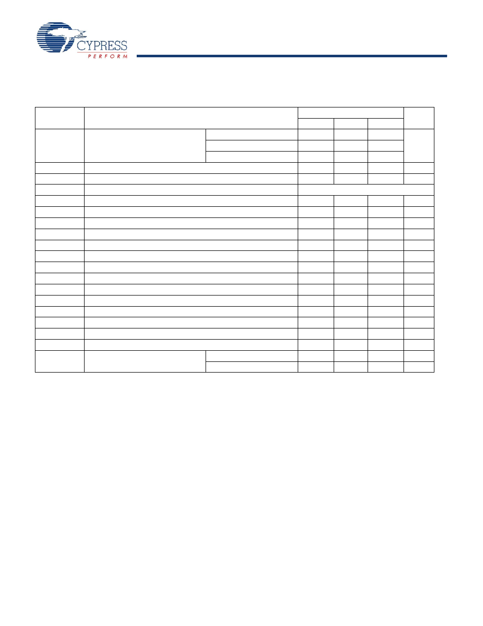
Switching Characteristics – 7 Option
Over the Operating Range
Parameter
Description
CY7B9911V-7
Unit
Min
Typ
Max
f
NOM
Operating Clock
Frequency in MHz
FS = LOW
15
30
MHz
FS = MID
25
50
FS = HIGH
40
110
t
RPWH
REF Pulse Width HIGH
5.0
ns
t
RPWL
REF Pulse Width LOW
5.0
ns
t
U
Programmable Skew Unit
See
t
SKEWPR
Zero Output Matched Pair Skew (XQ0, XQ1)
0.1
0.25
ns
t
SKEW0
Zero Output Skew (All Outputs)
0.3
0.75
ns
t
SKEW1
Output Skew (Rise-Rise, Fall-Fall, Same Class Outputs)
0.6
1.0
ns
t
SKEW2
Output Skew (Rise-Fall, Nominal-Inverted, Divided-Divided)
1.0
1.5
ns
t
SKEW3
Output Skew (Rise-Rise, Fall-Fall, Different Class Outputs)
0.7
1.2
ns
t
SKEW4
Output Skew (Rise-Fall, Nominal-Divided, Divided-Inverted)
1.2
1.7
ns
t
DEV
Device-to-Device Skew
1.65
ns
t
PD
Propagation Delay, REF Rise to FB Rise
–0.7
0.0
+0.7
ns
t
ODCV
Output Duty Cycle Variation
–1.2
0.0
+1.2
ns
t
PWH
Output HIGH Time Deviation from 50%
3
ns
t
PWL
Output LOW Time Deviation from 50%
3.5
ns
t
ORISE
Output Rise Time
0.15
1.5
2.5
ns
t
OFALL
Output Fall Time
0.15
1.5
2.5
ns
t
LOCK
PLL Lock Time
0.5
ms
t
JR
Cycle-to-Cycle Output
Jitter
RMS
25
ps
Peak
[12]
100
200
ps
Notes
11. Test measurement levels for the CY7B9911V are TTL levels (1.5V to 1.5V). Test conditions assume signal transition times of 2 ns or less and output loading
as shown in the
unless otherwise specified.
12. Guaranteed by statistical correlation. Tested initially and after any design or process changes that may affect these parameters.
13. SKEW is defined as the time between the earliest and the latest output transition among all outputs for which the same tU delay is selected when all are loaded
with 30 pF and terminated with 50
Ω to VCC/2 (CY7B9911V).
14. tSKEWPR is defined as the skew between a pair of outputs (XQ0 and XQ1) when all eight outputs are selected for 0tU.
15. tSKEW0 is defined as the skew between outputs when they are selected for 0tU. Other outputs are divided or inverted but not shifted.
16. CL=0 pF. For CL=30 pF, tSKEW0=0.35 ns.
17. There are three classes of outputs: Nominal (multiple of tU delay), Inverted (4Q0 and 4Q1 only with 4F0 = 4F1 = HIGH), and Divided (3Qx and 4Qx only in
Divide-by-2 or Divide-by-4 mode).
18. tDEV is the output-to-output skew between any two devices operating under the same conditions (VCC ambient temperature, air flow, and so on.)
19. tODCV is the deviation of the output from a 50% duty cycle. Output pulse width variations are included in tSKEW2 and tSKEW4 specifications.
20. Specified with outputs loaded with 30 pF for the CY7B9911V-5 and -7 devices. Devices are terminated through 50
Ω to VCC/2.tPWH is measured at 2.0V. tPWL
is measured at 0.8V.
21. tORISE and tOFALL measured between 0.8V and 2.0V.
22. tLOCK is the time that is required before synchronization is achieved. This specification is valid only after VCC is stable and within normal operating limits. This
parameter is measured from the application of a new signal or frequency at REF or FB until tPD is within specified limits.