Connector pinouts, Pci-104 header (p1), Jtag programming header (p2) – Connect Tech 104 User Manual
Page 9: Spi flash programming header (p3), Table 4: jtag programming header pinout (p2), Table 5: spi flash programming header pinout (p3)

Connect Tech FreeForm/PCI-104 User Manual
Revision 0.00
9
Connector Pinouts
PCI-104 Header (P1)
Refer to
JTAG Programming Header (P2)
Use P2 to configure the FPGA via JTAG. Refer to
Programming the FPGA
for more information.
Power pins are for voltage reference only; they do not provide power to the configuration
circuitry.
Note that the FPGA can always be programmed via JTAG, regardless of the
J1
configuration
setting.
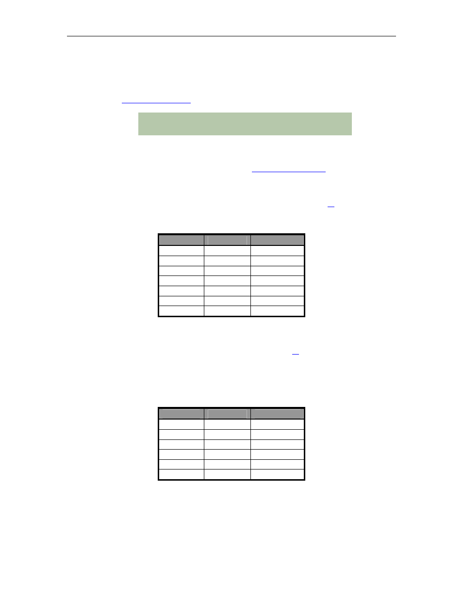
Table 4: JTAG Programming Header Pinout (P2)
Pin
Signal
Direction
1
TRST
Input
2
TMS
Input
3
TDI
Input
4
TDO
Output
5
TCK
Input
6
GND
Reference
7
3.3V
Reference
SPI Flash Programming Header (P3)
P3 may be used to directly program the SPI flash, providing that
J1
is set correctly to the tri-state
FPGA position. The power pins are for voltage reference only. They do not provide power to the
configuration circuitry.
Table 5: SPI Flash Programming Header Pinout (P3)
Pin
Signal
Direction
1
SPI_CSN
Input
2
SPI_MOSI
Input
3
SPI_MISO
Output
4
SPI_CLK
Input
5
GND
Reference
6
3.3V
Reference
Note: P1 must be connected to a PCI-104 stack supplying
both 3.3V and 5V
