Application schematic – Cypress CY25566 User Manual
Page 6
CY25566
Document #: 38-07429 Rev. *B
Page 6 of 9
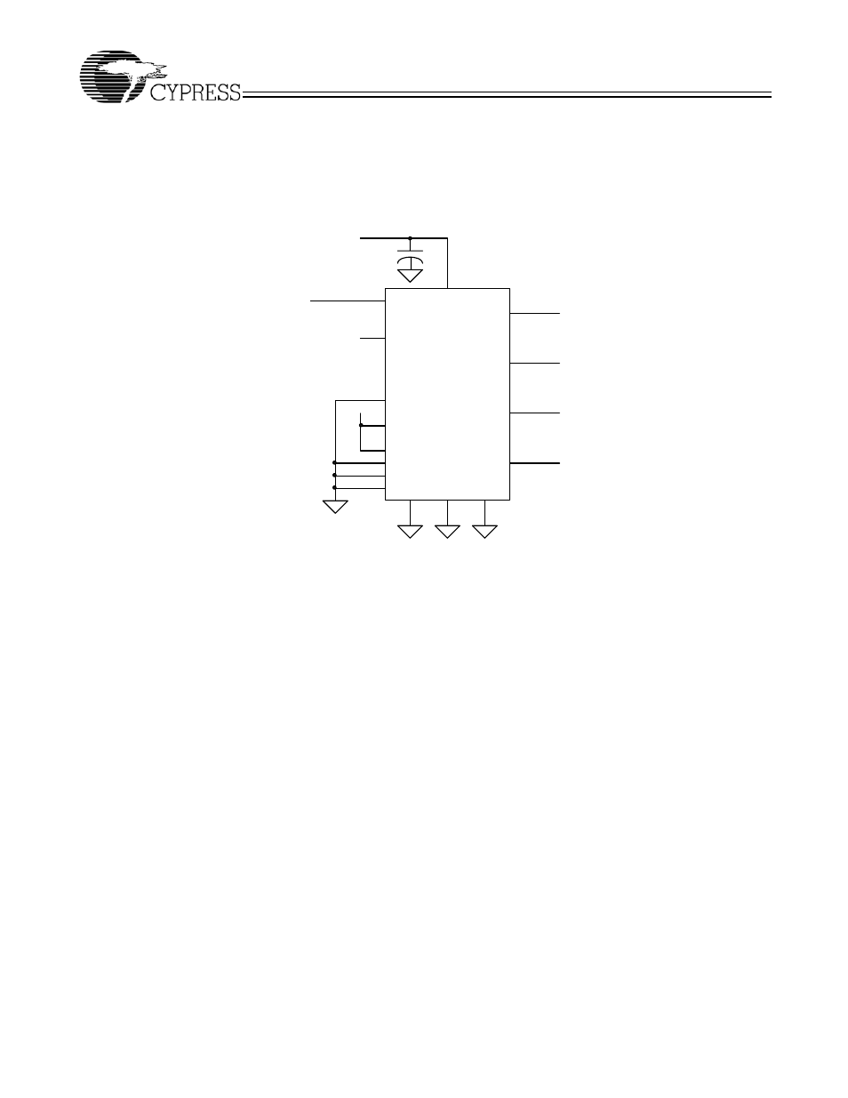
Application Schematic
In this example, the CY25566 is being driven by a 75-MHz
reference clock.
S0 = 0 and S1 = 0 are programmed to select a BW of 2.5%.
(Refer to Table 1 and 2.)
S2 = 0 and S3 = 1 are programmed to select the Group 2
range.
V
DD
= 3.30 VDC.
SSCLK1a = 75 MHz @ 2.5% center spread modulation.
SSCLK1b = 75 MHz @ 2.5% center spread modulation.
SSCLK 2 = 37.5 MHz @ 2.5% center spread modulation.
REFOUT = 37.5 MHz non-modulated clock.
CY25566
XIN/CLKIN
XOUT
REFOFF
SSCC
S2
S3
S1
S0
REFOUT
SSCLK2
SSCLK1a
SSCLK1b
VDD
VSS
VSS
VSS
VDD
VDD
75 MHz Clock source
REFOUT
SSCLK2
SSCLK1a
SSCLK1b
0.1 uF
1
2
3
16
10
7
6
12
8
13
9
5
11
14
15
4
Figure 4. Application Schematic