Come-mbt10 / pinout list – Kontron COMe-mBT10 User Manual
Page 51
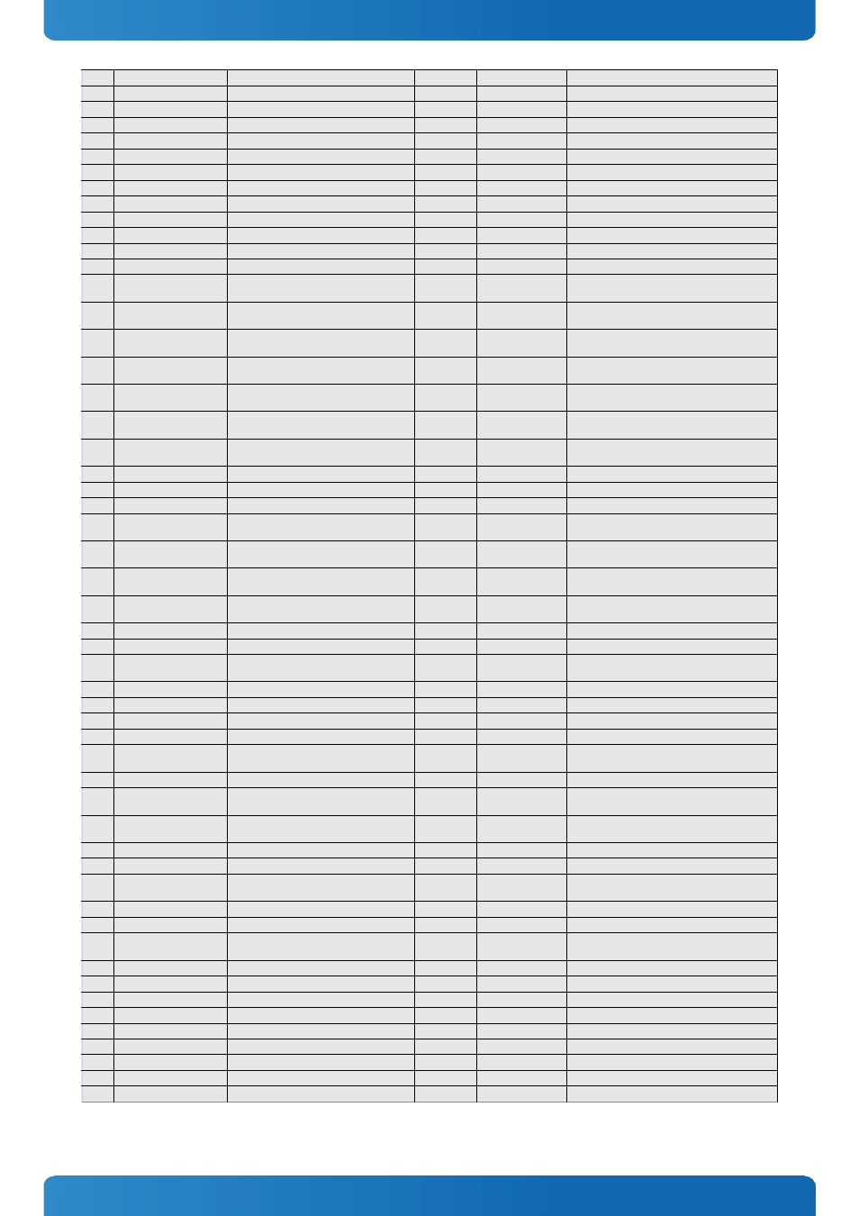
COMe-mBT10 / Pinout List
A58
PCIE_TX3+
PCI Express Lane 3 Transmit +
DP-O
-
-
A59
PCIE_TX3-
PCI Express Lane 3 Transmit -
DP-O
-
-
A60
GND
Power Ground
PWR GND
-
-
A61
PCIE_TX2+
PCI Express Lane 2 Transmit +
DP-O
-
-
A62
PCIE_TX2-
PCI Express Lane 2 Transmit -
DP-O
-
-
A63
GPI1/SD_DATA1
General Purpose Input 1 (shared SD DATA1)
I-3.3
PU 100k 3.3V (S0)
-
A64
PCIE_TX1+
PCI Express Lane 1 Transmit +
DP-O
-
-
A65
PCIE_TX1-
PCI Express Lane 1 Transmit -
DP-O
-
-
A66
GND
Power Ground
PWR GND
-
-
A67
GPI2/SD_DATA2
General Purpose Input 2 (shared SD DATA2)
I-3.3
PU 100k 3.3V (S0)
-
A68
PCIE_TX0+
PCI Express Lane 0 Transmit +
DP-O
-
-
A69
PCIE_TX0-
PCI Express Lane 0 Transmit -
DP-O
-
-
A70
GND
Power Ground
PWR GND
-
-
A71
LVDS_A0+/eDP_TX2+
LVDS Channel A Data0 + (shared eDP TX2+)
DP-O
-
configuration as eDP_TX0+ in customised article
version possible
A72
LVDS_A0-/eDP_TX2-
LVDS Channel A Data0 - (shared eDP TX2-)
DP-O
-
configuration as eDP_TX0- in customised article
version possible
A73
LVDS_A1+/eDP_TX1+
LVDS Channel A Data1 + (shared eDP TX1+)
DP-O
-
configuration as eDP_TX1+ in customised article
version possible
A74
LVDS_A1-/eDP_TX1-
LVDS Channel A Data1 - (shared eDP TX1-)
DP-O
-
configuration as eDP_TX1- in customised article
version possible
A75
LVDS_A2+/eDP_TX0+
LVDS Channel A Data2 + (shared eDP TX0+)
DP-O
-
configuration as eDP_TX2+ in customised article
version possible
A76
LVDS_A2-/eDP_TX0-
LVDS Channel A Data2 - (shared eDP TX0-)
DP-O
-
configuration as eDP_TX2- in customised article
version possible
A77
LVDS/eDP_VDD_EN
LVDS (or eDP) Panel Power Control
O-3.3
PD 100k
configuration as eDP_VDD_EN in customised
article version possible
A78
LVDS_A3+
LVDS Channel A Data3 +
DP-O
-
-
A79
LVDS_A3-
LVDS Channel A Data3 -
DP-O
-
-
A80
GND
Power Ground
PWR GND
-
-
A81
LVDS_A_CK+/eDP_TX3+
LVDS Channel A Clock (shared eDP TX3+)
DP-O
-
configuration as eDP_TX3+ in customised article
version possible
A82
LVDS_A_CK-/eDP_TX3-
LVDS Channel A Clock - (shared eDP TX3-)
DP-O
-
configuration as eDP_TX3- in customised article
version possible
A83
LVDS_I2C_CK/eDP_AUX+
LVDS Data Channel Clock (shared eDP AUX+) I/O-3.3
PU 2k21 3.3V (S0)
configuration as eDP_AUX+ in customised article
version possible
A84
LVDS_I2C_DAT/eDP_AUX- LVDS Data Channel Data (shared eDP AUX-)
I/O-3.3
PU 2k21 3.3V (S0)
configuration as eDP_AUX- in customised article
version possible
A85
GPI3/SD_DATA3
General Purpose Input 3 (shared SD DATA3)
I-3.3
PU 100k 3.3V (S0)
-
A86
RSVD
Reserved for future use
nc
-
-
A87
RSVD/eDP_HPD
Reserved (shared eDP hot plug detection)
nc/I-3.3
-
configuration as eDP_HPD in customised article
version possible
A88
PCIE_CLK_REF+
Reference PCI Express Clock +
DP-O
-
-
A89
PCIE_CLK_REF-
Reference PCI Express Clock -
DP-O
-
-
A90
GND
Power Ground
PWR GND
-
-
A91
SPI_POWER
3.3V Power Output Pin for external SPI flash O-3.3
-
might be powered during suspend
A92
SPI_MISO
SPI Master IN Slave OUT
I-3.3
PD 20k in CPU (SPI) All SPI signals are tri-stated with 20k ohm CPU
internal weak pull-up until reset is deasserted
A93
GPO0/SD_CLK
General Purpose Output 0 (shared SD clock) O-3.3
PD 100k
-
A94
SPI_CLK
SPI Clock
O-3.3
PD 20k in CPU (SPI) All SPI signals are tri-stated with 20k ohm CPU
internal weak pull-up until reset is deasserted
A95
SPI_MOSI
SPI Master Out Slave In
O-3.3
PD 20k in CPU (SPI) All SPI signals are tri-stated with 20k ohm CPU
internal weak pull-up until reset is deasserted
A96
TPM_PP
TPM Physical Presence
nc
-
TPM_PP not supported by used TPM
A97
TYPE10#
Pull down for TYPE 10 module
nc
PD 47k
-
A98
SER0_TX
Serial Port 0 TXD
O-3.3
-
20V protection circuit implemented on module, PD
on carrier board needed for proper operation
A99
SER0_RX
Serial Port 0 RXD
I-5T
PU 47k 3.3V (S0)
20V protection circuit implemented on module
A100 GND
Power Ground
PWR GND
-
-
A101 SER1_TX
Serial Port 1 TXD
O-3.3
-
20V protection circuit implemented on module, PD
on carrier board needed for proper operation
A102 SER1_RX
Serial Port 1 RXD
I-5T
PU 47k 3.3V (S0)
20V protection circuit implemented on module
A103 LID#
LID Switch Input
I-3.3
PU 47k 3.3V (S5)
20V protection circuit implemented on module
A104 VCC_12V
Main Input Voltage (8.5-20V)
PWR 8.5-20V -
-
A105 VCC_12V
Main Input Voltage (8.5-20V)
PWR 8.5-20V -
-
A106 VCC_12V
Main Input Voltage (8.5-20V)
PWR 8.5-20V -
-
A107 VCC_12V
Main Input Voltage (8.5-20V)
PWR 8.5-20V -
-
A108 VCC_12V
Main Input Voltage (8.5-20V)
PWR 8.5-20V -
-
A109 VCC_12V
Main Input Voltage (8.5-20V)
PWR 8.5-20V -
-
A110 GND
Power Ground
PWR GND
-
-
51