3 memory and cache optimizations, Memory and cache optimizations – Kontron MSM800BEV V101 BIOS User Manual
Page 43

Geode LX800 / LX900
/ BIOS
www.kontron.com
41
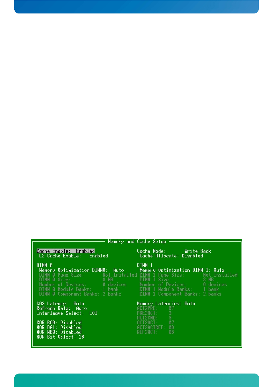
7.3.3 Memory and Cache Optimizations
The Memory and Cache Optimizations screen should be removed from all systems before shipping to the customer.
Incorrectly configuring the memory can render the system unable to boot and it may be necessary to short circuit the
CMOS to get the system to boot.
Cache Enable: Allows the configuration of the system Cache to either Enabled or Disabled.
Cache Mode: Allows selection of the Cache mode, either Write-Back or Write-Through.
DIMM 0 or 1:
Memory Optimization DIMM 0 or 1: Allows the memory to be configured by Auto or Manual. If Auto is
selected then Page Size, Size, Module Banks, and Component Banks will be grayed out.
DIMM 0 or 1 Page Size: Options are Not Installed, 1, 2, 4, 8, 16 kB.
DIMM 0 or 1 Size: Allows configuration of the Memory size to 8MB, 16MB, 32MB, 64MB, 128MB,
256MB, or 512MB. (alternately: 8, 16, 32, 64, 128, 256 or 512MByte.
Module Banks: Allows configuration of the number of module banks; options are 1 or 2.
DIMM Component Banks: Allows configuration of the component banks; options are 2 or 4.
CAS Latency (SDR/DDR): Allows the configuration of CAS (Column Address Select) latency. The options are
Auto, 2CLK/1.5CLK, 3CLK/2CLK, 4CLK/ 2.5CLK, 5CLK/3CLK or 6CLK/NA.
DDR/SDR: Allows the selection of the memory type; options include Auto, DDR and SDR.
Refresh rate: Allows the setting of the memory refresh rate. Options include: auto, 3us, 7us, 15us, 31us,
62us and 125us.
Interleave selection: Allows setting of the interleaving to either LOI (Low Order Interleaving) or HOI (High
Order Interleaving).
XOR MB0, BA0 or BA1: Options are Enable or Disable of the XORing of module bank BA1or BA0 with upper
GLIU address bit.
Memory Latencies: Allows manual or auto configuration of the memory latencies.
ACT2PRE: ACT to PRE period (tRAS). Minimum number of clocks from the ACT to PRE commands on
the same component bank.
PRE2ACT: Pre to ACT period (tRP). Minimum number of SDROM clocks between PRE and ACT
commands.
ACT2CMD: Delay time from ACT to Read/Write (tRCD). Minimum number of SDRAM clocks between
ACT and Read/Write Commands.
ACT2ACT: ACT(0) to ACT(1) period (tRRD). Minimum number of SDRAM clocks between ACT and ACT
commands to two different component banks within the same module bank.
REF2ACT: Refresh to Activity Delay (tRFC). Minimum number of SDCLKS 90-31 between refresh and
next command, usually inactive.
