6 board diagrams, 1 functional block diagram, Board diagrams - 7 – Kontron CP6003-RC User Manual
Page 27: Functional block diagram - 7, Cp6003-ra/rc introduction, Gen . intel ® co re ™ i 7, Intel ® qm 67
CP6003-RA/RC
Introduction
ID 1046-3890, Rev. 1.0
Page 1 - 7
P R E L I M I N A R Y
1.6
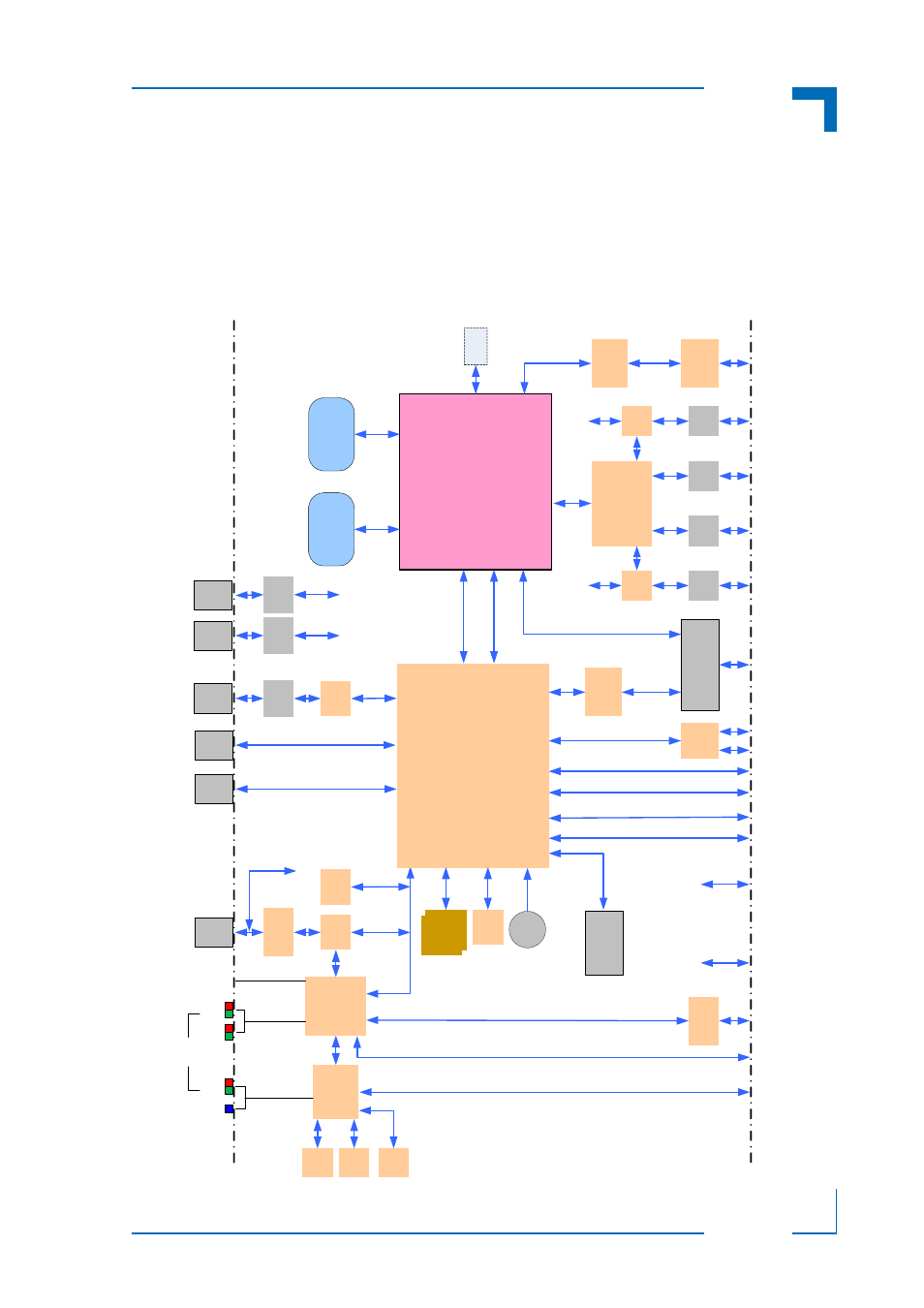
Board Diagrams
The following diagrams provide additional information concerning board functionality and
component layout.
1.6.1
Functional Block Diagram
Figure 1-1:
CP6003-RA/RC Functional Block Diagram
Fro
n
t Pa
ne
l
(CP
6
00
3
-RA
)
cP
CI
2x
USB
D
ebu
g
DMI
2.0
4x
US
B
4x
SAT
A
SIO
Te
m
p
.
Sens
e
GbE
PC
I 64
/66
M
H
z
3.3
V
/
5
V
VIO
TH/
WD
HS
IP
MB
CO
MA
RJ
4
5
Ho
t
Sw
ap
SA
TA
F
la
s
h M
o
du
le
VGA C
R
T
1
000
BT
RJ
-4
5
PC
I /
PC
IX
64/
13
3 M
H
z
Gb
E
M
ag.
DD
R3 w
/ EC
C
sol
d
er
ed
m
e
mo
ry
C
h
a
nnel A
2
nd
gen
.
Intel
®
Co
re
™ i
7
DDR
3
DDR
3
Intel
®
QM
67
USB
DMI
SM
B
SPI
PC
Ie
FD
I
DP
XD
P
FD
I
PC
I
64
/6
6
M
H
z
2x
HDMI
/DV
I
ET
H
2xD
P
SATA
HD
A
HDA
M
ag.
D
DR3 w
/
EC
C
sol
d
e
red
me
mo
ry
C
han
nel B
PC
Ie
to
PC
I
M
ag.
1000
BT
RJ
-4
5
Ma
g
.
Re
a
r I
/O
J
4
VG
A
DP
RS
T
IPM
I
100
0
B
T
RJ
-4
5
Ma
g.
to R
ear
I
/O
PCI
e
x4
COMB
CO
MA
Gb
E
PH
Y
Quad
GbE
Co
n
tro
lle
r
to
F
ro
n
t I
/O
to
VGA
Sw
it
ch
FPGA
Bo
ar
d
Con
tro
l
IPMI
Co
ntro
ller
EEP
EEP
Fl
a
s
h
FR
U
fr
om
Quad
GbE
Co
n
tro
lle
r
PC
Ie
x4
uE
F
I
BIO
S
Fl
ash
TPM
LP
C
LP
C
LED
s
to
Fr
ont I
/O
R
S
-422/
R
S
-232
PCI
e
x4
GP
DMI
FDI
PC
Ie
PC
Ie
(on r
e
q
uest
)
Bat
.
RTC
GP
IO
3.
3V
VG
A/
CRT
VGA
U
S
B
Gb
E
Sw
it
c
h
Gb
E
Swit
c
h
Ma
g
.
Ma
g
.
to
F
ro
n
t
I/
O
PC
Ie
to
PC
I
PM
C
/XM
C
PC
I
/ PC
IX
or
XM
C
PC
Ie x
8
DP
to
HDMI /
DV
I
PC
Ie x
8
PC
Ie
GbE
Gb
E
J3
J3
PI
C
M
G 2
.16
J3
R
S
-232
I
2
C