Charles Industries 31929E User Manual
Page 4
Section 319–29E–202
4
The 3192–9E input current is highly dependent on application. Those applications that require the 3192–9E to
power a customer’s CSU will require a greater input current.
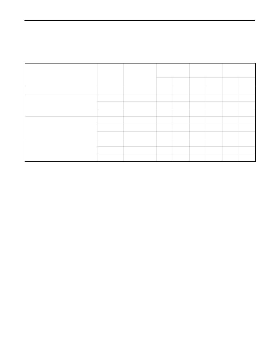
Table 1 shows input current and heat release versus the equivalent series simplex resistance (at 60mA) present
on the CI side of the unit.
Table 1. 3192–9E Power Consumption and Heat Release
Typical Application
Option S1
Position
Equivalent
External
Simplex
–42.5 Volt
Battery
48.0 Volt Bat-
tery
56.0 Volt Bat-
tery
Simplex
Resistance
I
W
I
W
I
W
Non-CPE Powering
S1 = LP
N/A
0.07
2.86
0.06
2.87
0.06
3.00
Sealing Current Only
S1 = SC
0 Ohms
0.08
3.35
0.07
3.53
0.07
3.77
S1 = PWR
200 Ohms
0.10
2.91
0.08
3.02
0.07
3.12
S1 = PWR
400 Ohms
0.11
3.04
0.10
3.12
0.08
3.18
Powering Co-located 24V CSU
S1 = PWR
600 Ohms
0.13
3.09
0.11
3.12
0.10
3.13
S1 = PWR
800 Ohms
0.14
3.18
0.13
3.13
0.11
3.14
S1 = PWR
1000 Ohms
0.16
3.22
0.14
3.18
0.13
3.15
Powering Co-located 68V CSU
S1 = PWR
1200 Ohms
0.18
3.32
0.16
3.22
0.14
3.22
S1 = PWR
1400 Ohms
0.20
3.45
0.18
3.23
0.16
3.28
S1 = PWR
1600 Ohms
0.22
3.55
0.20
3.38
0.18
3.39
Note:
W = Heat release in watts
I = Input current in amps
2.3
Maintenance Loopback
The 3192–9E provides a signal path Loopback feature, which can be used to differentiate circuit problems on ei-
ther side of the network interface.
The 3192–9E will respond to Loopback control codes in either SF or ESF protocols. SF control codes are re-
ceived as 5 or 6 bit inband repeating patterns, while ESF codes are via 16 bit messages in the ESF framing data
link. The operation of this feature is automatic, that is, when the unit is passing unframed or SF framed traffic it
will recognized the 5 or 6 bit inband SF Loop codes, when the unit is passing ESF traffic it will only recognize the
ESF data link Loopback control codes.
When the 3192–9E is in the maintenance loopback state, it will send an AIS (all ones) signal toward the Custom-
er Interface.
3.
CIRCUIT DESCRIPTION
Refer to Figure 4, the 3192–9E Block Diagram, Figure 5, the 3192–9E State Table, and Figure 6, Front Panel
Features and Options Location, when reading the following circuit description.