Pin configurations, Ssop, Top view – Cypress CY14B101K User Manual
Page 2: Is used) v
CY14B101K
Document Number: 001-06401 Rev. *I
Page 2 of 28
Pin Configurations
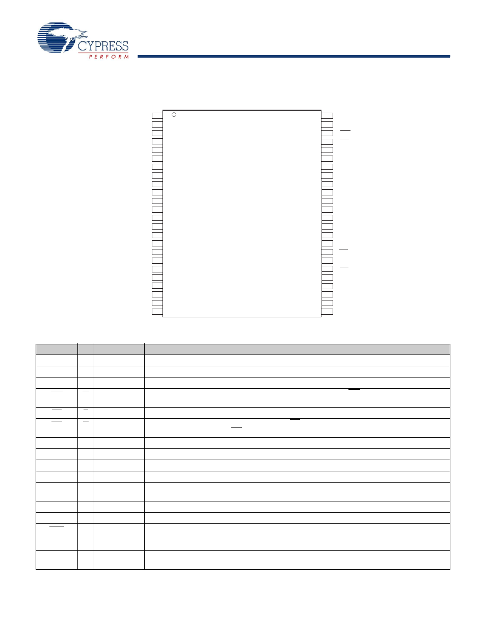
Figure 1. 48-Pin SSOP
Table 1. Pin Definitions
Pin Name
Alt
IO Type
Description
A
0
– A
16
Input
Address Inputs. Used to select one of the 131,072 bytes of the nvSRAM.
DQ0 – DQ7
Input Output
Bidirectional Data IO Lines. Used as input or output lines depending on operation
NC
No Connect
No Connects. This pin is not connected to the die
WE
W
Input
Write Enable Input, Active LOW. When the chip is enabled and WE is LOW, data on the IO pins
is written to the specific address location.
CE
E
Input
Chip Enable Input, Active LOW. When LOW, selects the chip. When HIGH, deselects the chip.
OE
G
Input
Output Enable, Active LOW. The active low OE input enables the data output buffers during
READ cycles. Deasserting OE high causes the IO pins to tri-state.
X
1
Output
Crystal Connection Drives crystal on start up.
X
2
Input
Crystal Connection for 32.768 kHz crystal.
V
RTCcap
Power Supply Capacitor Supplied Backup RTC Supply Voltage. (Left unconnected if V
RTCbat
is used)
V
RTCbat
Power Supply Battery Supplied Backup RTC Supply Voltage. (Left unconnected if V
RTCcap
is used)
INT
Output
Interrupt Output. Program to respond to the clock alarm, the watchdog timer, and the power
monitor. Programmable to either active HIGH (push or pull) or LOW (open drain).
V
SS
Ground
Ground for the Device. Must be connected to ground of the system.
V
CC
Power Supply Power Supply Inputs to the Device.
HSB
Input Output
Hardware Store Busy. When LOW this output indicates a Hardware Store is in progress. When
pulled LOW external to the chip it initiates a nonvolatile STORE operation. A weak internal pull up
resistor keeps this pin HIGH if not connected (connection optional).
V
CAP
Power Supply AutoStore™ Capacitor. Supplies power to nvSRAM during power loss to store data from SRAM
to nonvolatile elements.
V
CAP
A
16
A
14
A
12
A
7
A
6
A
5
A
4
V
CC
A
15
HSB
WE
A
13
A
8
A
9
A
11
OE
A
10
DQ
DQ7
6
DQ5
CE
DQ4
DQ3
1
2
3
4
5
6
7
8
9
10
11
12
13
14
15
16
17
18
19
20
21
22
23
24
48
47
46
45
44
43
42
41
40
39
38
37
36
35
34
33
32
31
30
29
28
27
26
25
INT
NC
NC
NC
V
SS
NC
DQ0
A
3
A
2
A
1
A
0
DQ1
DQ2
NC
NC
NC
NC
V
SS
NC
V
CC
48-SSOP
Top View
(Not To Scale)
V
RTCbat
x
1
x
2
V
RTCcap