Multi-phase design guide, Programming synchronization delay – Vicor PI33XX-XX Multi-Phase Design Guide User Manual
Page 3
vicorpower.com Rev 1.0
Cool-Power
®
800 735.6200 11/2012 Page 3 of 4
Multi-Phase Design Guide
Programming Synchronization Delay
The PI33XX-2X provides an I
2
C
TM
Standard Mode
digital interface that enables the user to
program phase delays. This is a one-time
programmable option to the device. To set a
delay, the user needs to assign a unique Device
Address (see Table 2) to wake up the device
during
programming.
Then
send
the
synchronization delay address (21h) and the
delay data (OEh) while adhering to I
2
C protocols
and Figure 4 sequencing.
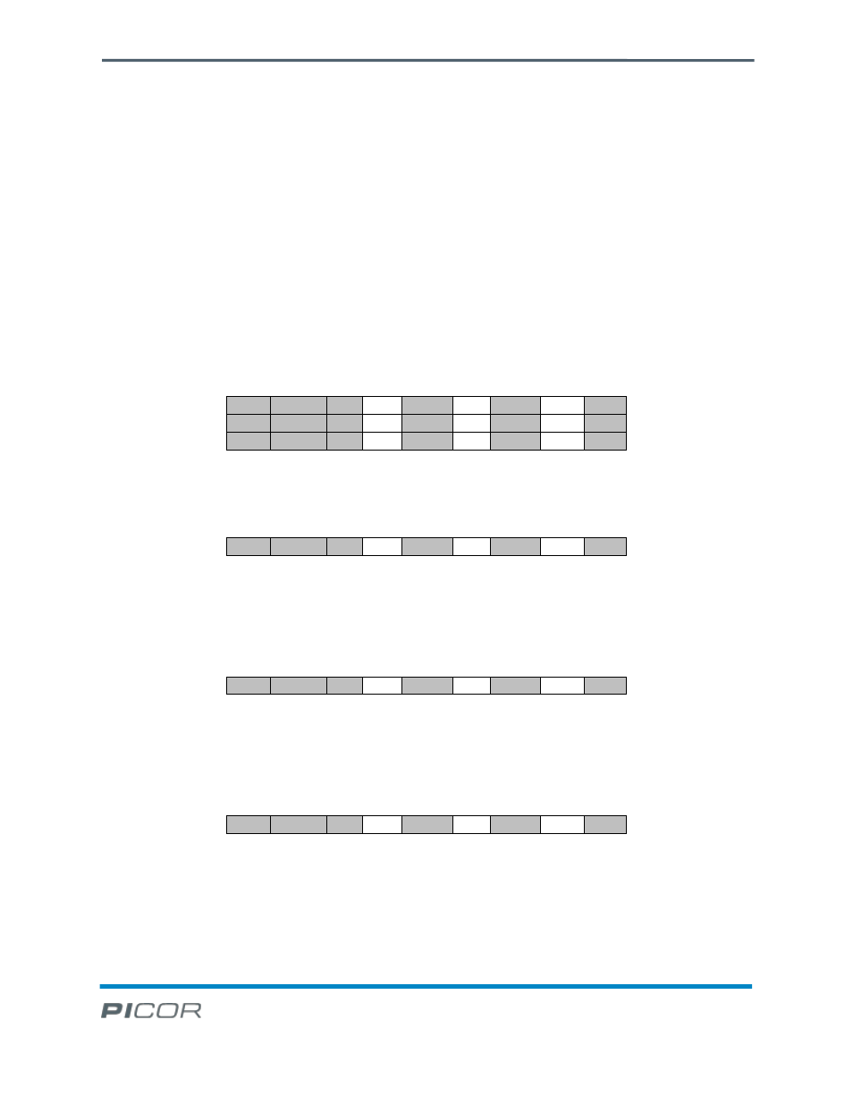
The following figure demonstrates the proper
steps to program a single phase-delay. The
device address is determined by the user and
the synchronization delay is provided in Table 1.
The device address is represented as XXh (Bold)
in Figure 6. Because this process in not
reversible, it is important to follow all steps in
Figure 4.
1) Clear all Registers to 00h with the device enabled
Start
Addr.
Device
Wr
Ack
Addr.
Reg
Ack
Data
Ack
Stop
S
XXh
1
0
20h
0
00h
0
P
S
XXh
1
0
21h
0
00h
0
P
S
XXh
1
0
22h
0
00h
0
P
2) Enter Test Mode 5
Start
Adr.
Device
Wr
Ack
Adr.
Reg
Ack
Data
Ack
Stop
S
XXh
1
0
18h
0
05h
0
P
3) Disable then Re-enable the Device (Enable Pin)
4) Set Desired Delay
Start
Adr.
Device
Wr
Ack
Adr.
Reg
Ack
Data
Delay
Ack
Stop
S
XXh
1
0
21h
0
0Eh
0
P
5) Disable Device (Enable Pin)
6) Return to Test Mode 0
Start
Adr.
Device
Wr
Ack
Adr.
Reg
Ack
Data
Ack
Stop
S
XXh
1
0
18h
0
00h
0
P
7) Repeat 1); Clearing all Registers
8) Enable Device (Enable Pin); Programming is Complete
Figure 4 - Showing the 8 Steps Required to Program a Single 1/3 Phase Delay