Vicor PI2121-EVAL1 Full-Function Active ORing Evaluation Board User Manual
Page 6
Picor Corporation • www.picorpower.com
PI2121-EVAL1 User Guide Rev 1.1 Page 6 of 12
3.0 Blanking timer setup:
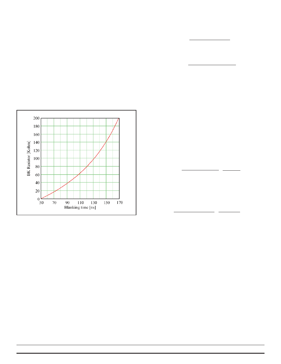
3.1 The blanking timer provides noise filtering for
typical switching power conversion that might
cause premature reverse current detection by
masking the reverse fault condition. The shortest
blanking time is 50 ns when the BK pin is
connected to ground. Connecting an external
resistor (R
BK
, reference designators R6 for SiP1 and
R13 for SiP2) between the BK pin and ground will
increase the blanking time as shown in Figure 5.
Where: R
BK
≤ 200 KΩ
Note: When BK is connected to VC for slave mode .
operation,then the blanking time will be 270 ns typically.
4.0 Auxiliary Power Supply (Vaux):
4.1 The PI2121 ORing solution has a separate input (VC)
that provides power to the control circuitry and
the internal gate driver. An internal voltage regulator
(VC) clamps the VC voltage to 15.5 V typically.
4.2 Connect an independent power source to the Vaux
inputs of PI2121-EVAL1 Evaluation Board to supply
power to the VC inputs. The Vaux voltage should be
5 V higher than Vin (redundant power source output
voltage) to fully enhance the internal MOSFET.
4.3 10
Ω bias resistors (Rbias, reference designators R7
and R14) are installed on the PI2121-EVAL1 board
between each Vaux input and VC pin of the
PI2121 solution.
4.4 If Vaux is higher than the Clamp voltage, 15.5 V
typical, the Rbias value has to be changed using
the following equations:
4.4.1 Select the value of Rbias using the following
equation:
Rbias =
Vaux
min
– VC
clampMAX
IC
max
4.4.2
Calculate Rbias maximum power dissipation:
Pd
Rbias
=
(Vaux
max
– VC
clampMIN
)
2
Rbias
Where:
Vaux
min
: Vaux minimum voltage
Vaux
max
: Vaux maximum voltage
VC
ClampMAX
: Maximum controller
clamp voltage, 16.0 V
VC
ClampMIN
: Minimum controller
clamp voltage, 14.0 V
IC
max
: Controller maximum bias current,
use 4.2 mA
4.4.3 For example, if the minimum Vaux = 22 V
and the maximum Vaux = 28 V
Rbias =
Vaux
min
– VC
clampMAX
=
22 V–16 V
= 1.429 K
Ω
IC
max
4.2 mA
,
use 1.43 K
Ω 1% resistor
Pd
Rbias
= (Vaux
max
– VC
clampMIN
)
2
= (28 V–14.0 V)
2
=137 mW
Rbias 1.43 K
Ω
Note: Minimize the resistor value for low Vaux voltage
levels to avoid a voltage drop that may reduce the VC
voltage lower than required to drive the gate of the
internal MOSFET.
Figure 5 –BK Resistor selection versus Blanking Time