AOC P/N : 41A50-144 User Manual
Page 55
54
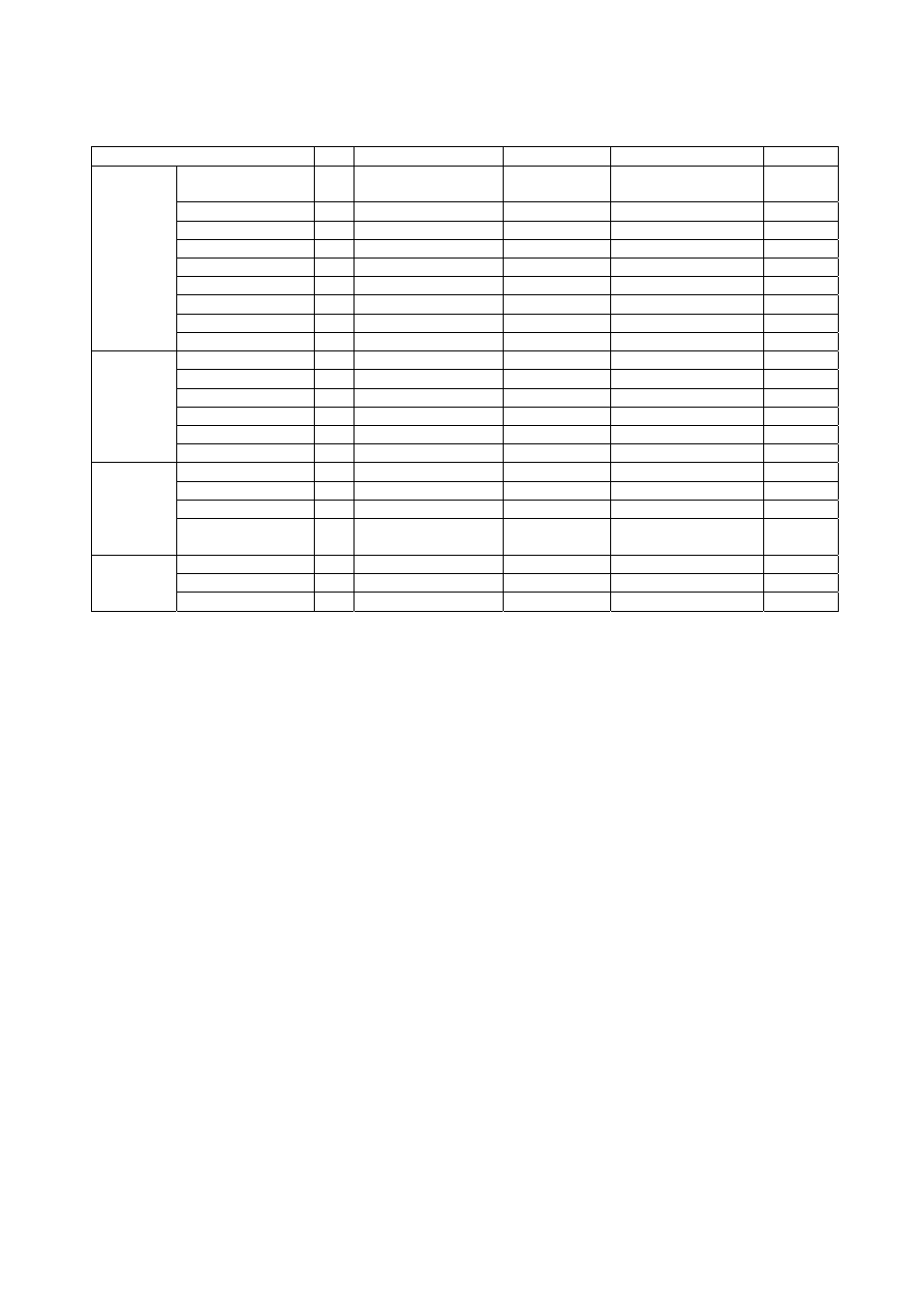
Table 13. gmZAN1 TFT Panel Interface Timing
Signal Name
Min
Typical
Max
Unit
Period t1
0
16.67
2048
-
lines
ms
Frequency
60
-
Hz
Front porch
t2
0
2048
lines
Back porch
t3
0
2048
lines
Pulse width
t4
0
2048
lines
PdispE t5
0
Panel
height
2048
lines
Disp. Start from VS t6
0
2048
lines
PVS set up tp PHS
t18
1
2048
PCLK *1
PVS
PVS hold from PHS t19
1
2048
PCLK *1
Period
t7
0
2048 [1024
PCLK *1
Front porch
t8
0
2048
PCLK *1
Back porch
t9
0
2048
PCLK *1
Pulse width
t10
0
2048
PCLK *1
PdispE
t11
0
Panel width
2048 [1024]
PCLK *1
PHS
Disp. Start fom HS t12
0
2048
PCLK *1
Frequency t13
120
[60]
MHz
Clock (H) *2
t14
DCLK/2-3 [DCLK-3]
DCLK/2-2 [DCLK-2] ns
Clock (L) *2
t15
DCLK/2-3 [DCLK-3]
DCLK/2-2 [DCLK-2] ns
PCLKA,
PCLKB*4
Type
-
One
pxl/clock
[two pxl/clock]
-
Set up *3
t16
DCLK/2-5 [DCLK-5]
DCLK/2-2 [DCLK-2] ns
Hold *3
t17
DCLK/2-5 [DCLK-5]
DCLK/2-2 [DCLK-2] ns
Data
width
3 bits
18 bits [36 bits] 24 bits [48 bits]
bits/pixel
NOTE: Numbers in [ ] are for two pixels/clock mode.
NOTE: The drive current of the panel interface signals is programmable as shown in Table 1. The drive current is to be
programmed through the API upon chip initialization. Output current is programmable from 2 mA to 20mA in increments of 2 mA.
Drive strength should be programmed to match the load presented by the cable and input of the panel. Values shown are based on a
loading of 20pF and a drive strength of 8 mA.
NOTE *1: The PCLK is the panel shift clock.
NOTE *2: The DCLK stands for Destination Clock (DCLK) period. Is equal to:
-PCLK period in one pixel/clock mode,
-twice the PCLK period in two pixels/clock mode.
NOTE *3: The setup/hold time spec. for PCLK also applies to PHS and PdispE. The setup time (t16) and the hold time (t17) listed
in this table are for the case in which no clock-to-data skew is added. The PVS/PHS/PdispE/Pdata signals are asserted on
the rising edge of the PCLK. The polarity of the PCLK and its skew are programmable. Clock to Data skew can be
adjusted in sixteen 800-ps increments. In combination with the PCLK polarity inversion, the clock-to-data phase can be
adjusted in total of 31 steps.
NOTE *4: The polarity of the PCLKA and the PCLKB are independently programmable.
The micro controller must have all the timing parameters of the panel used for the monitor. The parameters are to be
stored in a non-volatile memory. As can be seen from this table, the wide range of timing programmability of the
gmZAN1 panel interface makes it possible to support various kinds of panels known today: