An356, Alternative configuration, 1 resistor configuration – Cirrus Logic AN356 User Manual
Page 2: R1 v, R2 v, R1 ------------------------------------- v, 79k ω
AN356
2
AN356REV1
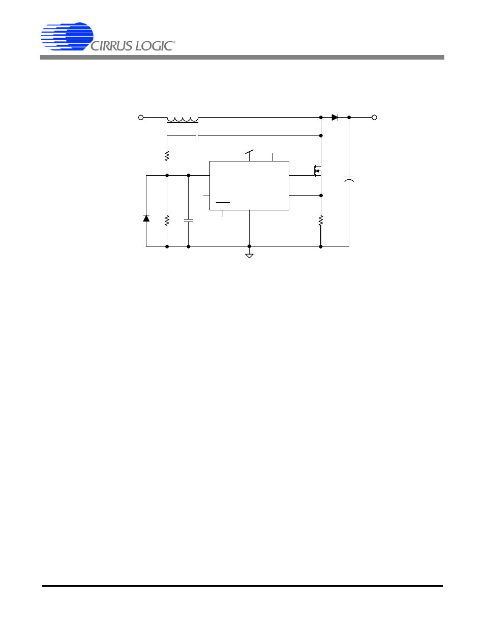
3. Alternative Configuration
It is possible to implement ZCD with a resistor divider from the drain of the PFC MOSFET. See Figure 2.
Figure 2. ZCD Alternative Implementation
At lighter loads, the resistor divider circuit may not pull the ZCD pin to its trigger threshold (low) as the ringing voltage itself drifts
away from zero volts. This can cause the drive to turn on while there is still a voltage across the drain to source of the Boost
MOSFET. Using a 47 pF capacitor in series with resistor R1, the issue of DC drift on the drain waveform is removed. The value
of the capacitor is minimized to prevent additional capacitive switching losses.
3.1 Resistor Configuration
The maximum current that can be drawn by the ZCD pin is I
zcd
= 1mA. Set a maximum voltage of 5 V for V
zcd
, with the voltage
on the MOSFET drain = 460 V.
Select R1 to be a standard value of 475 k
Ω.
Select R2 to be a standard value of 4.75 k
Ω.
Due to internal comparator design, the maximum external capacitor is 33 pF, as shown. This acts as a low-pass filter for high-
frequency switching noise. Values above this should not be used.
The addition of a Schottky diode is required to prevent negative voltages on the ZCD pin from exceeding -0.5 V. See Fig 3.
R1
R2
R
cs
8
1
Boost Diode
Boost
FET
CS1501
CS1601
GD
ZCD
IFB
GND
CS
IAC
VDD
L
B
6
3
5
7
4
V
DD
STBY
2
V
rect
V
link
33pF
47pF
500 V
Low Voltage
Schottky
R1
V
drain
V
zcd
–
(
)
I
zcd
-------------------------------------
455k
Ω
=
=
[Eq.1]
R2
V
drain
V
zcd
–
(
)
R1
------------------------------------- V
zcd
⋅
4.79k
Ω
=
=
[Eq.2]