Cirrus logic, inc, Cobranet™ ev-2, Rev. 2.1 34 – Cirrus Logic EV2 User Manual
Page 34: Clock buffers, Clock buffers optional vcxo
Rev. 2.1
34
CobraNet™ EV-2
1
2
34
A
B
C
D
4
3
2
1
D
C
B
A
C
o
braN
et (T
M
) E
valuation B
oard - O
p
tional V
C
XO
and clock buffers.
E
2500 55th Street
Sui
te 210
T
itle
:
File:
EV
2_V
CX
O
.Sch
69
19-O
ct-2004
Date:
Sheet
of
Engineer: Bill Lowe
www.
peakaudi
o.
com
www.
ci
rrus.
com
Size:
Num
b
er:
Revision:
A
Cirrus Logic, Inc.
B
o
ulder, C
O
80301
GND
C
606
.1S
FS512_O
U
T
FS512_IN
VC
1
OUT
3
GND
2
VCC
4
U
600
24.576M
H
Z
V
C
X
O
B
600
.1S
GND
R
606
10K
P1S
GND
VCC_+3
VCC_+3
1
2
3
U
601A
74LV
X
86S
4
5
6
U
601B
74LV
X
86S
9
10
8
U
601C
74LV
X
86S
12
13
11
U
601D
74LV
X
86S
VCC
14
GND
7
U
601E
74LV
X
86S
GND
FS512_EV
GND
VCC_+3
B
601
.1S
GND
VCC_+3
FS512_IN
FS512_O
U
T
R
603
464P1S
SSI_CLK
FS1_OUT
2
3
1
U
510A
74LV
X
125A
12
11
13
U
510D
74LV
X
125A
5
6
4
U
510B
74LV
X
125A
SSI_CLK_IN
SSI_CLK
9
8
10
U
510C
74LV
X
125A
AES_BCLK
AES_BCLK
FS1_IN
AES_FS1
FS1_OUT
AES_FS1
B
500
.1S
VCC_+3
GND
GND
GND
GND
GND
VCC
14
GND
7
U
501E
74LV
X
125A
2
3
1
U
501A
74LV
X
125A
12
11
13
U
501D
74LV
X
125A
VCC_+3
GND
GND
B
501
.1S
GND
FS512_CLK
FS512_CLK
MC
L
K
MC
L
K
VCC
14
GND
7
U
510E
74LV
X
125A
SSI_CLK_IN
FS1_IN
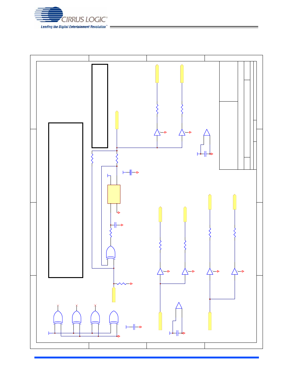
Clock buffers
Clock buffers
Optional VCXO
The V
C
X
O
circuit provides an example of a circuit that w
ill reduce jitter on the
master clock. In the EV
-2 application jitter is low
enough w
h
ere this circuit does
not improve the jitter performance significantly. The end user, because of long
trace lengths or running the master clock through other components such as gates
or FPG
A
s, may w
ant to consider implementing a jitter attenuation circuit such as
this one.
Without VCXO populate R501 and not R602.
With VCXO populate R602 and not R501.
R
511
51.1P1S
R
512
51.1P1S
R
515
51.1P1S
R
514
51.1P1S
R
502
51.1P1S
R
503
51.1P1S
R
602
51.1P1S
R
501
51.1P1S