An258 – Cirrus Logic AN258 User Manual
Page 5
AN258
AN258REV2
5
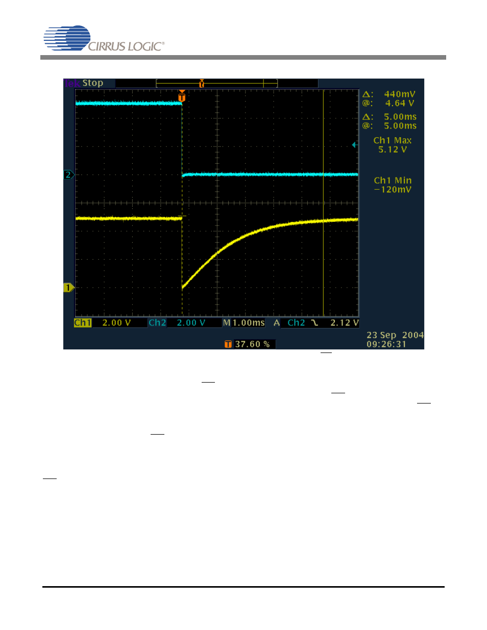
Figure 4. Oscilloscope View of the RC Circuit at the MR Pin
This figure shows channel 1, the output of the Schmitt-trigger inverter in Circuit 1, going low and staying
low. Channel 2 shows the voltage at the MR pin of the voltage monitor IC. Initially, C1 is charged by R1
but once the Schmitt-trigger inverter goes low, it causes a logic zero on the MR pin. C1 then starts charg-
ing through the pull-up resistor inside the voltage monitor IC. This causes the critical pulse on the MR pin
and keeps the voltage monitor IC from continually asserting a POR. The values for C1 and R1 and the
pull up inside the voltage monitor IC are not critical but must form a long enough period to satisfy the min-
imum input duration on the MR pin. In the case of the MAX708, this value is 125 ns. Figure 4 indicates
that this condition is easily satisfied.
In ciruit 2, resistor R4 should not be populated for normal operation. If circuit 2 is removed, location R4
must be populated with a zero-ohm resistor or solder short. R4 will connect the push button directly to the
MR pin.
Jumper J1 is installed by default. If using a debugger, it may be desired to prevent the restart circuit from
resetting the board. In that case, remove J1 for debugging.