An229 – Cirrus Logic AN229 User Manual
Page 3
AN229
3
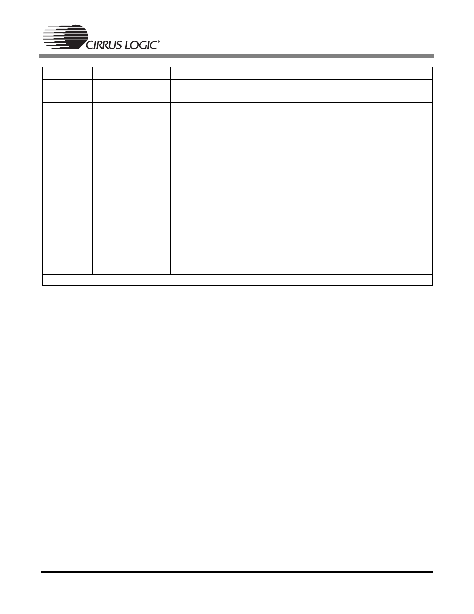
Pin Number CS8405A Pin Name CS8406 Pin Name Differences
2
VL2+
TEST
See “CS8406 Test Pins” on page 1.
6
VD+
VD
See “Power Supply” on page 1.
7
DGND4
TEST
See “CS8406 Test Pins” on page 1.
8
DGND3
TEST
See “CS8406 Test Pins” on page 1.
20
VL3+
HWCK0
Pins 20 and 27 set the OMCK clock ratio for the
CS8406. Setting both pins to VL (the recommended
setting from the CS8405A datasheet) or both pins to
GND will cause the clock ratio to be 256*Fs, the only
mode available for the CS8405A.
21
OMCK
OMCK
CS8405A OMCK clock ratio is 256*Fs.
CS8406 OMCK clock ratios can be 128*Fs, 256*Fs, or
512*Fs, set by HWCK[0:1].
23
VL+
VL
For both parts, the VL supply can operate at 3.3 V
or 5.0 V.
27
VL4+
HWCK1
Pins 20 and 27 set the OMCK clock ratio for the
CS8406. Setting both pins to VL (the recommended
setting from the CS8405A datasheet) or both pins to
GND will cause the clock ratio to be 256*Fs, the only
mode available for the CS8405A.
Pins 1, 3, 4, 5, 9, 10, 11, 12, 13, 14, 15, 16, 17, 18, 19, 22, 24, 25, 26, and 28 have the same functions on both parts.
Table 3. Hardware Mode Comparison