An229 – Cirrus Logic AN229 User Manual
Page 2
AN229
2
6. Output Resistance
The typical output resistance of the transmitter pins changed from the CS8405A to the CS8406.
The value of the external series resistor placed on the transmitter pins should be modified appro-
priately to account for this change. See the latest CS8406 datasheet for details on selecting the
value of the external resistor.
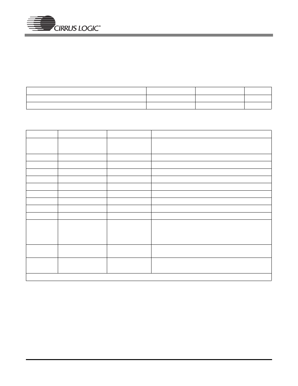
Table 1. Transmitter Output Resistance
Parameter
VL = 3.3 V
VL = 5 V
Unit
TXP/TXN CS8405A Output Resistance
40
26
Ω
TXP/TXN CS8406 Output Resistance
33.5
26.5
Ω
Pin Number CS8405A Pin Name CS8406 Pin Name Differences
1
SDA / CDOUT
SDA / CDOUT
CS8405A I
2
C
TM
is only supported at VL+ = 5.0 V.
CS8406 allows I
2
C operation at VL = 3.3 V or 5.0 V.
5
DGND2
TEST
See “CS8406 Test Pins” on page 1.
6
VD+
VD
See “Power Supply” on page 1.
7
DGND4
TEST
See “CS8406 Test Pins” on page 1.
8
DGND3
TEST
See “CS8406 Test Pins” on page 1.
10
NC1
TEST
See “CS8406 Test Pins” on page 1.
11
NC2
TEST
See “CS8406 Test Pins” on page 1.
16
NC3
TEST
See “CS8406 Test Pins” on page 1.
17
NC4
TEST
See “CS8406 Test Pins” on page 1.
18
NC5
TEST
See “CS8406 Test Pins” on page 1.
21
OMCK
OMCK
CS8405A OMCK clock ratios can be 256*Fs, 384*Fs,
or 512*Fs.
CS8406 OMCK clock ratios can be 128*Fs, 256*Fs,
384*Fs, or 512*Fs.
23
VL+
VL
For both parts, the VL supply can operate at 3.3 V
or 5.0 V.
28
SCL / CCLK
SCL / CCLK
CS8405A I
2
C is only supported at VL+ = 5.0 V.
CS8406 allows I
2
C operation at VL = 3.3 V or 5.0 V.
Pins 2, 3, 4, 9, 12, 13, 14, 15, 19, 20, 22, 24, 25, 26, and 27 have the same functions on both parts.
Table 2. Software Mode Comparison