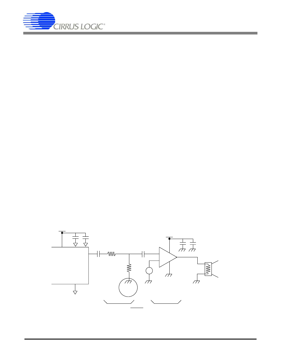
2 car-kit guidelines, Figure 19. speaker driver implementation, An168 – Cirrus Logic AN168 User Manual
Page 26: 1 +5va/agnd components, 2 +5vd/dgnd components
AN168
26
AN168REV2
2) Decoupling and loading capacitors should be
placed as close as possible to the pins they de-
couple (AVDD, AGND, DVDD, DGND, MB,
CLKI, CLKO), with the smaller-valued capac-
itor closest to the pin.
3) The traces between the MB pin and the decou-
pling capacitors connected to it should be short,
shielded with ground plane, and located far
from potentially interfering signals.
1.6.2
Car-Kit guidelines
Cellular car kits typically have three power
networks: +12VBATT/BATTGND,
+5VD/DGND, and +5VA/AGND.
Components powered from a particular power
network should have ground connections to the
ground associated with that power network. For
example, the CS6422 should be powered from
+5VA and its ground pins, including power supply
decoupling capacitor grounds and signal grounds,
should tie to AGND.
The one exception to this is that the attenuator
resistor in the resistor divider between AO and the
speaker driver should be tied to the ground of the
speaker driver, typically BATTGND if the speaker
driver is powered from the +12V battery source.
This prevents the speaker driver from amplifying
noise caused by potential differences between
AGND and BATT GND.
Following are listed the power networks and
components associated with each network.
1.6.2.1 +5VA/AGND Components
1) CS6422, AVDD, DVDD, AGND, DGND, de-
coupling capacitors, crystal loading capacitors,
signal R’s and C’s with the exception of the at-
tenuator resistor in the voltage divider between
AO and the speaker driver input.
2) Op-amps and analog circuitry between the cell
phone and the CS6422’s NO and NI pins.
1.6.2.2 +5VD/DGND Components
1) Microcontroller
2) Additional +5V control logic circuitry
Note: If the CS6422 and the microcontroller are
powered from the same +5V regulator, +5VA
should be derived from the regulator output
(+5VD) through a ferrite bead.
R
1
R
2
+
AO
Gain = +40 dB
+
AGND
BATT
GND
BATT
GND
BATT
GND
BATT
GND
10 µF
10 µF
+5 VA
+12 V
BATT GND
+
-
+
+
4
Ω
Speaker
Gain (dB) = 20 log ( )
R
2
R
1
+ R
2
CS6422
Figure 19. Speaker Driver Implementation