Cdb5529, Using the evaluation board – Cirrus Logic CDB5529 User Manual
Page 5
CDB5529
DS246DB1 5
Table 1 lists the RS-232 commands used to com-
municate between the PC and the microcontroller.
To develop additional code to communicate to the
evaluation board via RS-232, the following ap-
plies: to write to an internal ADC register, choose
the appropriate write command byte (See Table 1),
and transmit it LSB first. Then, transmit the three
data bytes, lowest order byte (bits 7-0) first, with
the LSB of each byte transmitted first. These three
data bytes provide the 24-bits of information to be
written to the desired register. To read from an in-
ternal register, choose the appropriate read com-
mand byte and transmit it LSB first. Then, the
microcontroller automatically acquires the ADC’s
register contents and returns the 24-bits of informa-
tion. The returned data is transmitted lowest order
byte first with the LSB of each byte transmitted
first.
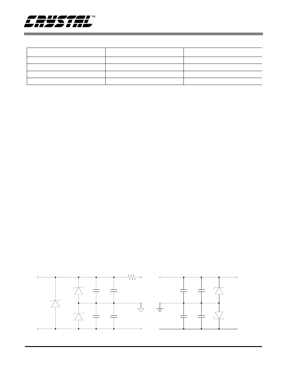
The CS5529 A/D converter is designed to operate
from a single +5V or a dual ±2.5V analog supply.
Figure 3 illustrates the power supply connections to
the evaluation board. The +2.5/5V Analog supplies
the positive analog section of the evaluation board,
the LT1019 and the ADC. The -2.5V Analog sup-
plies the negative. HDR8 (see Figure 1) can be used
to bypass VA- to ground. The +5V Digital supplies
the digital section of the evaluation board. It pow-
ers the 80C51, the reset circuitry, and the RS-232
interface circuitry.
Using the Evaluation Board
The CS5529 is a highly integrated ADC. It contains
coarse/fine charge buffers and programmable out-
put word rates (OWR). The buffers provide charge
to the modulator reducing the dynamic current de-
mand from the signal being digitized and from the
external reference. The ADC’s digital filter allows
the user to select output word rates (OWR’s) from
1.88 Hz up to 101.1 Hz (assuming a 32.768 kHz
clock). 303 Hz output word rates can be attained
when a 100kHz clock source is used. Since the
CS5529 has such a high degree of integration and
flexibility, the CS5529 data sheet should be read
thoroughly before and consulted during the use of
the CDB5529.
Register Read Command Byte Write Command Byte
Offset Register 0x90 (H) 0x80 (H)
Gain Register 0x92 (H) 0x82 (H)
Configuration Register 0x94 (H) 0x84 (H)
Conversion Data Register 0x96 (H) ---
Table 1. Microcontroller Command via RS-232
+2.5V / 5V Analog
-2.5V Analog
Z2
P6KE6V8P
+
C6
47µF
C20
0.1µF
Z3
P6KE6V8P
+
C5
47µF
C14
0.1µF
Z4
P6KE6V8P
+
C8
47µF
C12
0.1µF
+5V / 3.3V A/D Digital
AGND DGND
Z5
P6KE6V8P
+
C8
47µF
C12
0.1µF
To µC VD+
Z1
P6KE6V8P
To HDR3
To HDR8
R21
10
Ω
+5V Digital
Figure 3. Power Supplies