An75 – Cirrus Logic AN75 User Manual
Page 2
AN75
2
AN75REV2
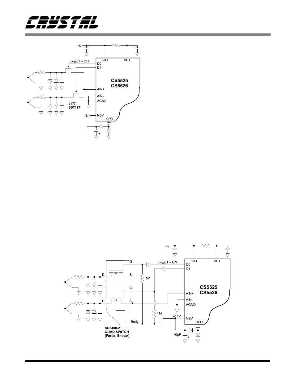
gate junction. When ON, the J177 (SST177) exhib-
its a resistance of 300 ohms maximum. If used to
switch signals less than ±250 mV, the leakage cur-
rent (25 °C) will be sub-picoamps.
Figure 3 illustrates an example of using an en-
hancement mode transistor switch as an analog
switch. The SD5400-2 quad DMOS switch is illus-
trated (the SD5000-2, SD5200-2, and SD5300-2
series are similar). The diode-resistor drive combi-
nation on the gate of the SD5400-2 allows the gate
to go to -0.6 V when the DO-D3 logic drive from
the CS5525/CS5526 is low. The -0.6V gate drive
shuts off the transistor with adequate gate drive to
ensure very high off resistance. When the D0-D3
output drive is high, the transistor is on with a resis-
tance less than 100
Ω
. Signals of ±1 V can readily
be passed by the switch.
Some analog switches are available which are de-
signed to function with supply voltages of ±5 V or
less. The Advanced Linear Devices ALD4201 quad
switch is used in Figure 4 (1/2 of device is shown)
for switching thermocouple signals. The switch is
operated from a +5 V supply and from the NBV
voltage (-2.1) used for the CS5525/CS5526. This is
acceptable as the supply current requirement of the
ALD4201 is only a microampere. Leakage currents
for the ALD4201 are stated to remain below 500
pA over the industrial temperature range. On resis-
tance over the industrial temperature range with a
total supply of +5V or more is less than 300
Ω
.
This application note illustrates the flexibility of
using the CS5525/CS5526 digital output pins to
control analog switches and multiplexers. While all
the circuits introduced have illustrated the CS5525/
CS5526 being used in thermocouple applications,
the device can be used for bridge transducers as
well.
Figure 2. CS5525/CS5526 Controls P-Channel
JFETs as analog switches.
Figure 3. CS5525/CS5526 Controls N-Channel DMOS transistors as analog switches.