Cirrus Logic AN75 User Manual
Cirrus Logic Hardware

MAY ‘97
AN75REV2
1
Copyright
Crystal Semiconductor Corporation 1997
(All Rights Reserved)
Crystal Semiconductor Corporation
P.O. Box 17847, Austin, Texas 78760
(512) 445 7222 FAX: (512) 445 7581
http://www.crystal.com
AN75
Application Note
Using the CS5525/CS5526 in Multiplexed Applications
By Jerome Johnston
The CS5525/CS5526 A/D converter is optimized
for the measurement of thermocouples. It is de-
signed with a single analog input, but includes four
digital output pins to control analog switches and
multiplexers. The performance characteristics of
an analog switch or multiplexer in a thermocouple
digitizer application are important because of the
typical protection circuitry which is included in the
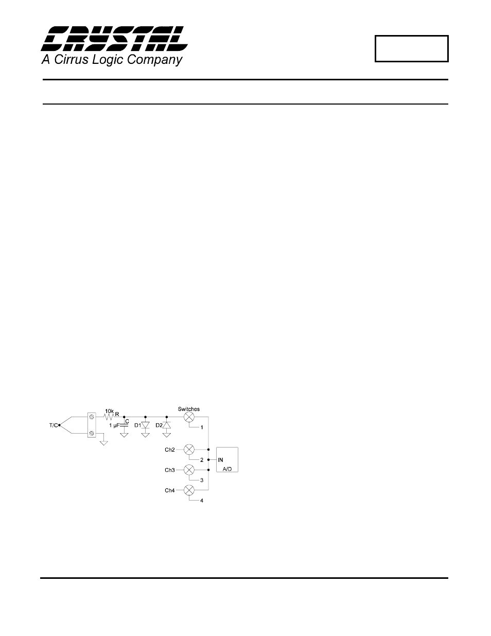
signal path. Figure 1 illustrates a multiplexed ther-
mocouple circuit which includes input protection.
Resistor R, capacitor C, and diodes D1 and D2 pro-
vide input protection for the analog switch and the
A/D converter. Input protection guards against
ESD (Electro-Static Discharge), high voltage
glitches which can get coupled into long thermo-
couple leads in an industrial environment, and in-
correct connections which can cause +24 volts to
become directly connected to the digitizer input
terminals.
To achieve sufficient protection, the input protec-
tion resistor is usually 10 K
Ω
or greater. This resis-
tance can introduce measurement errors if leakage
currents in the circuitry are large. Even small
changes in leakage currents can affect accuracy
since thermocouple output voltages change very
little for each degree of temperature change (typi-
cally between 6 µ V/°C and 80 µV/°C). Therefore,
leakage current from the analog switch or from the
input of the amplifier used to amplify the thermo-
couple signal can introduce significant errors if a
large protection resistor is used. A large value for
the protection resistor is desirable because the com-
bination of R and C also act as a low pass filter to
help reject 50/60 Hz. A large resistor value helps to
achieve a low frequency cutoff for the filter while
using a small capacitor value (many applications
use surface mounted components in which the
availability of surface mounted capacitors is limit-
ed to low values). The capacitor is usually a low
leakage device with a quality dielectric to achieve
low dielectric absorption.
Figure 2 illustrates the CS5525/CS5526 using the
p-channel J177 (or SST177 for surface mount)
JFET as an analog switch. The J177 has a maxi-
mum V
GS(off)
of 2.25 V, therefore a +5 V drive sig-
nal from one of the digital outputs from the
CS5525/CS5526 can turn it off (Driving the gate of
the JFET with only +3.0 volts will shut the J177 off
but it can exhibit more leakage current). When the
logic drive to the gate of the JFET is 0 V, the FET
will be turned on. It can safely handle input signals
of ±250 mV without forward biasing the channel to
Figure 1. Typical Thermocouple
Digitizer Input Circuitry
