Cirrus Logic AN158 User Manual
By keith coffey & jerome johnston, Input cvf (sampling) current
1
Copyright
Cirrus Logic, Inc. 1999
(All Rights Reserved)
P.O. Box 17847, Austin, Texas 78760
(512) 445 7222 FAX: (512) 445 7581
http://www.cirrus.com
AN158
Application Note
MEASURING HIGH VOLTAGES (5 TO 1,000 VOLTS) WITH
THE CS5521/23, CS5522/24/28, AND CS5525/26 A/D
CONVERTERS
By
Keith Coffey & Jerome Johnston
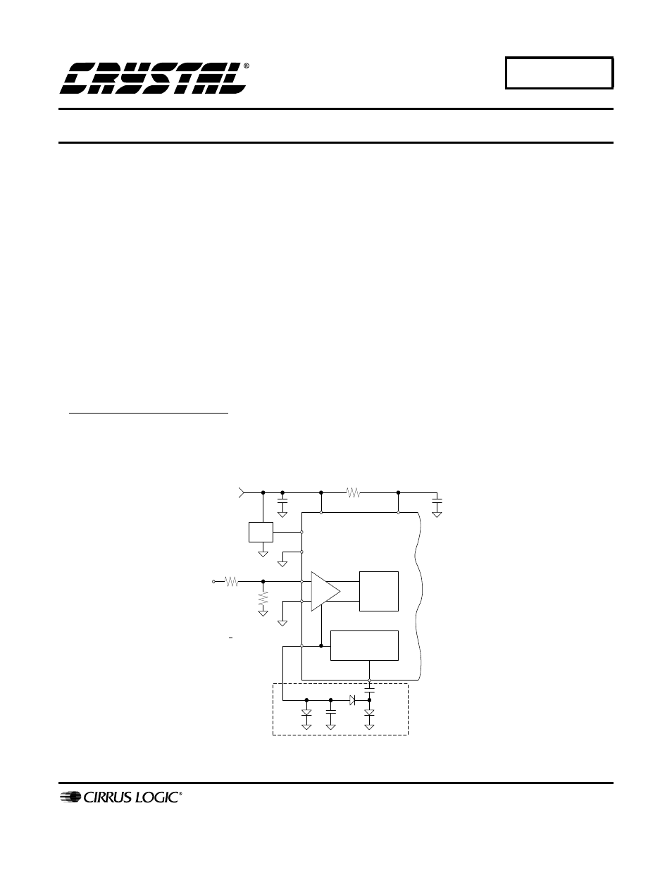
The CS5521/23, CS5522/24/28, and CS5525/26
1
A/D converters include a low input current (<300
pA input current over -40 to +85°C), chopper-sta-
bilized programmable gain instrumentation ampli-
fier (PGIA). A charge pump control loop is also
included on-chip to provide a negative supply to
the amplifier. This pump, which uses external com-
ponents, enables the amplifier to measure ground-
referenced signals even though the A/D is powered
from a single +5 V supply (see Figure 1).
This applications note discusses the features of the
amplifier and how it can be used to measure large
dc voltages.
INPUT CVF (SAMPLING) CURRENT
The programmable gain instrumentation amplifier
in the CS552x family is a CMOS, chopper-stabi-
1.The CS5529 is not included in this Application
Note because it does not contain an instrumentation
amplifier.
Voltage
Divider
PGIA set for
+ 100 mV
VIN
Charge Pump
Regulator
∆Σ
ADC
PGIA
+5 V
2.5 V
VA+
VREF+
VREF-
VD+
+
-
NBV
V
≈
-2.1 V
+
10
µ
F
0.033
µ
F
CPD
0.1
µ
F
10
Ω
0.1
µ
F
1N4148
1N4148
BAT85
Charge Pump
Circuitry
Figure 1. CS552X ADC with Charge Pump
AUG ‘99
AN158REV1