Cdb5381 – Cirrus Logic CDB5381 User Manual
Page 4
CDB5381
4
DS563DB1
* denotes default factory settings
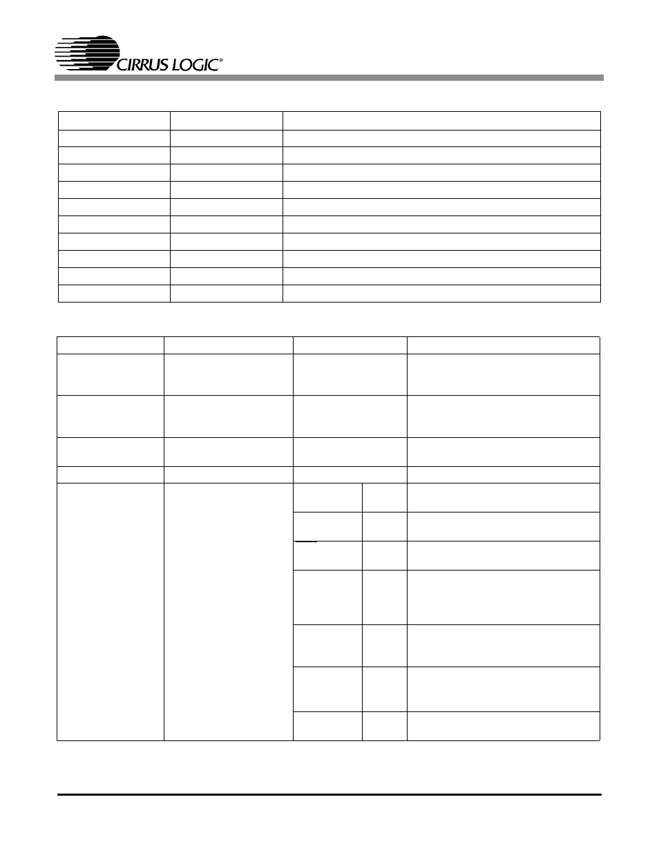
CONNECTOR
INPUT/OUTPUT
SIGNAL PRESENT
-12 V
Input
-12 V power for the input op-amps
+12 V
Input
+12 V power for the input op-amps
VD
Input
+3.3 V to +5 V power for the CS5381
VL
Input
+2.5 V to +5 V power for the CS5381
GND
Input
Ground connection from power supply
+5 V
Input
+ 5 Volt power
AINL
Input
Differential analog input left channel
AINR
Input
Differential analog input right channel
Optical Output
Output
Digital audio output
Coax Output
Output
Digital audio output
Table 1. System Connections
JUMPER/SWITCH
PURPOSE
POSITION
FUNCTION SELECTED
J7
VD Power Source
ADJ
*+3.3 V
+5 V
Power from the Binding Post (J3)
Power from the +3.3 V Regulator
Power from the +5V Supply
J8
VL Power Source
ADJ
*+3.3 V
+5 V
Power from the Binding Post (J4)
Power from the +3.3 V Regulator
Power from the +5 V Supply
J13
Input/Output for
clocks/data
-
-
S1
Reset for the CDB5381
-
-
S2
CDB5381 Configuration
M1/M0
Open
*Closed
Hi
Low
ADC
*Open
Closed
CS5381 in Master mode
CS5381 in Slave mode
HPF
Open
*Closed
High-pass filter is disabled
High-pass filter is enabled
DIV
Open
*Closed
MCLK is divided by two internally by the
CS5381
MCLK is not divided internally by the
CS5381
IO_HDR
Open
*Closed
Header J3 is an input for clocks
Header J3 is an output for clocks and
data
DIF
Open
*Closed
Digital interface format set to I
2
S
Digital interface format set to Left Justi-
fied
8406
Open
*Closed
CS8406 in Master mode
CS8406 in Slave mode
Table 2. CDB5381 Jumper and Switch Settings